


Other Parts Discussed in Thread: ADS8556
Supply voltages:
+5V for AVdd and +VIN -5V for HVSS and -VIN
+5V for AVdd
+3.3V for BVdd (digital supply)
I currently have the same test voltage (+2V) applied to all 6 channels of the ADS8556EVM kit (setup in HW + Parallel data mode). This helps to insure that all of the data bits (DB0 through DB15) stay at the same (or close to the same) value after a conversion read.
After I command a conversion, I wait for the BUSY interrupt. Then I read all 6 channels by:
1. Driving the !CS pin low
2. Toggling the !RD pin low, then high, 6 times (one per each channel read).
3. Driving the !CS pin back high
I took this screenshot (yellow trace shows the BUSY interrupt pulse being generated, Blue trace is directly on pin 64 of the ADS8556, which is DB15, the MSB output):
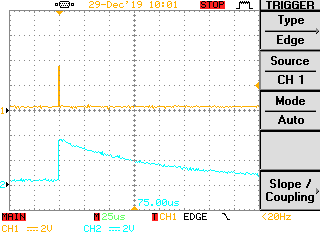
My test voltage means that the blue trace (MSB bit) should be HIGH, but it is obviously "sagging". I checked several of the digital output bits, and they all look like this exponentially decaying trace.
My question: why is the trace sagging? Shouldn't it remain high? This is causing my micro to read erratic output values.


