


Other Parts Discussed in Thread: ADS1299
Tool/software: Code Composer Studio
I used the MSP432P401R (MASTER) to initialize the ADS1299 and tried to read the ID, but the identification was 0x00, and I only entered 5 bytes of data in the CODE, but ran out 7 bytes. I do n’t know what happened
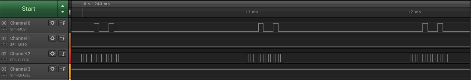
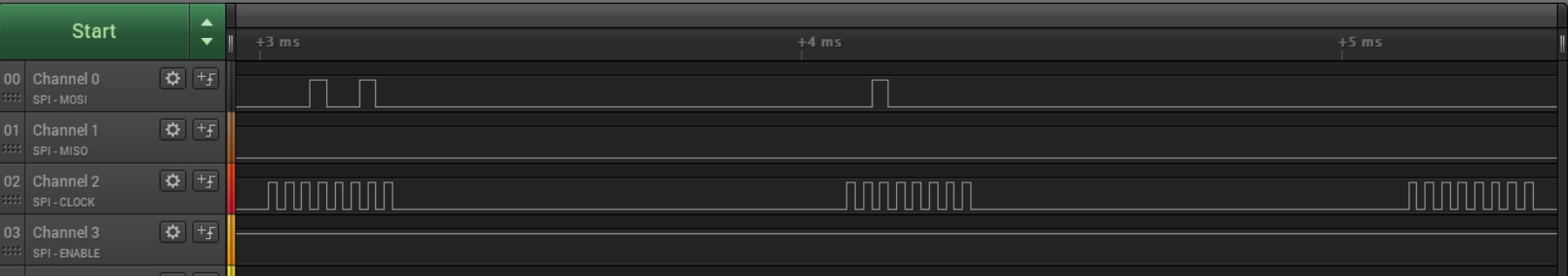
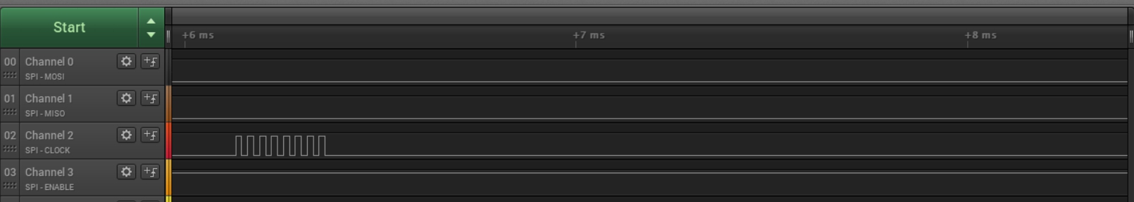
This picture is the overall logic analyzer signal diagram, CH0 is MOSI, CH1 is MISO, CH2 is CLOCK, CH3 is DRDY, CS I keep him constant low
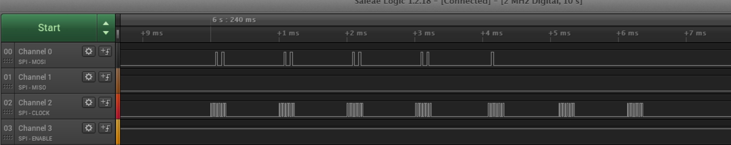
The following three pictures are enlarged views of the first picture, starting from the first byte in order.
/* DriverLib Includes */
#include <ti/devices/msp432p4xx/driverlib/driverlib.h>

/* Standard Includes */
#include <stdint.h>
#include <stdbool.h>
#define HZ  3000000UL
/* Statics */
static volatile uint8_t RXData = 0;
static uint8_t TXData = 0;
uint8_t A = 0;

int main(void)
{
    WDT_A->CTL = WDT_A_CTL_PW |             // Stop watchdog timer
             WDT_A_CTL_HOLD;

     P1->SEL0 |= BIT5 | BIT6 | BIT7;         // Set P1.5, P1.6, and P1.7 as
                                             // SPI pins functionality
     EUSCI_B0->CTLW0 |= EUSCI_B_CTLW0_SWRST; // Put eUSCI state machine in reset
     EUSCI_B0->CTLW0 = EUSCI_B_CTLW0_SWRST | // Remain eUSCI state machine in reset
             EUSCI_B_CTLW0_MST |             // Set as SPI master
             EUSCI_B_CTLW0_SYNC |            // Set as synchronous mode
             //EUSCI_B_CTLW0_CKPL |            // Set clock polarity low
             EUSCI_B_CTLW0_CKPH |            //Phase high
             EUSCI_B_CTLW0_MSB;              // MSB first

     EUSCI_B0->CTLW0 |= EUSCI_B_CTLW0_SSEL__ACLK; // ACLK
     EUSCI_B0->BRW = 0x01;                   // /2,fBitClock = fBRCLK/(UCBRx+1).
     EUSCI_B0->CTLW0 &= ~EUSCI_B_CTLW0_SWRST;// Initialize USCI state machine
  //   EUSCI_B0->IE |= EUSCI_B_IE_RXIE;        // Enable USCI_B0 RX interrupt
 /////////////////////////////////////////////////SPI INTERRUPT/////////////////////////////////////////////////////////////////////////////////
     __enable_irq();

     // Enable eUSCI_B0 interrupt in NVIC module
     NVIC->ISER[0] = 1 << ((EUSCIB0_IRQn) & 31);

     // Wake up on exit from ISR
     SCB->SCR &= ~SCB_SCR_SLEEPONEXIT_Msk;

     // Ensures SLEEPONEXIT takes effect immediately
     __DSB();


     P1->OUT &= ~BIT0;
     P1->DIR |= BIT0;                        // Set P1.0 LED

     P1->SEL0 |= BIT5 | BIT6 | BIT7;         // Set P1.5, P1.6, and P1.7 as
                                             // SPI pins functionality
 ///////////////////////////////////////////////////////////////////////////////////////////////////////////////////////////////
     /*TXData = 0x01;                          // Initialize TX data to 0x01
     while(1)
     {
        TXData++;
        spiTx(TXData);
        spiRx ();
     }*/

     //CS_Low();
     P3->DIR |= BIT0;
     P3->OUT ^= BIT0; //CS_Low
     __delay_cycles(HZ);
     P3->DIR |= BIT5;
     P3->OUT =  BIT5;       //CLKSEL High
     __delay_cycles(HZ/1000);

     P5->DIR |= BIT1;
     P5->OUT =  BIT1;       //PWDN High
     __delay_cycles(HZ);

     P2->DIR |= BIT7;
     P2->OUT = BIT7;      //RESET High
     __delay_cycles(HZ);


     P2->DIR |= BIT7;
     P2->OUT ^= BIT7;      //RESET LOW
     __delay_cycles(HZ);

     P2->DIR |= BIT7;
     P2->OUT = BIT7;      //RESET High
     __delay_cycles(HZ);


     TXData = 0x11;//SDATAC
     EUSCI_B0->IFG |= EUSCI_B_IFG_TXIFG;// Clear TXIFG flag
     EUSCI_B0->IE |= EUSCI_B_IE_TXIE;    // Enable TX interrupt

     TXData = 0x12;//RDATA
     EUSCI_B0->IFG |= EUSCI_B_IFG_TXIFG;// Clear TXIFG flag
     EUSCI_B0->IE |= EUSCI_B_IE_TXIE;    // Enable TX interrupt

     P2->DIR |= BIT6;
     P2->OUT |= BIT6;    //Set Start High

     A = spi_bmp183_read8(0x20);

     }


uint8_t spi_bmp183_read8(uint8_t reg) {


  // Make sure transmit buffer is clear
  while (!(SPI_getInterruptStatus(EUSCI_B0_BASE,EUSCI_B_SPI_TRANSMIT_INTERRUPT)));

  SPI_transmitData(EUSCI_B0_BASE, reg);                 // Transmit register address
  __delay_cycles(HZ/1000);
  // Send clock pulses.  This will push slave to send data to master on MISO line.
  SPI_transmitData(EUSCI_B0_BASE, 0x00);
  __delay_cycles(HZ/1000);
  SPI_transmitData(EUSCI_B0_BASE, 0x00);
  __delay_cycles(HZ/1000);
// Make sure transmit buffer is clear
  while (!(SPI_getInterruptStatus(EUSCI_B0_BASE,EUSCI_B_SPI_RECEIVE_INTERRUPT)));

  RXData = SPI_receiveData(EUSCI_B0_BASE);      // Pick up received byte in SPI receive data register

  return RXData;
}
void EUSCIB0_IRQHandler(void)
{
    if (EUSCI_B0->IFG & EUSCI_B_IFG_TXIFG)
    {
        EUSCI_B0->TXBUF = TXData;           // Transmit characters
        __delay_cycles(HZ/1000);
        //EUSCI_B0->TXBUF = 0x20;           // Transmit characters
        //__delay_cycles(HZ/100000);
        //EUSCI_B0->TXBUF = 0x00;           // Transmit characters
        //__delay_cycles(HZ/100000);
        EUSCI_B0->IE &= ~EUSCI_B__TXIE;

    }

}

