This thread has been locked.

If you have a related question, please click the "Ask a related question" button in the top right corner. The newly created question will be automatically linked to this question.

ADS1278: SPI interface timing characteristics and performance

Part Number: ADS1278

HI,

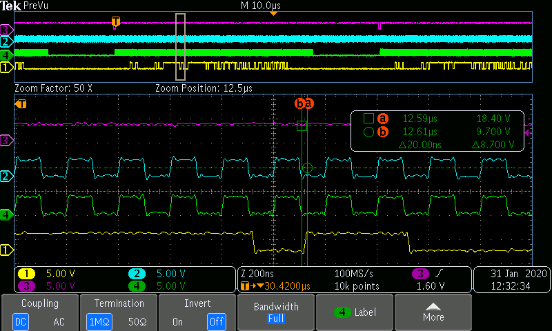
I have an issue in reading the data accurately when the SCLK / CLK is set to 20 MHz but reads accurately when clocked at 5 MHz.

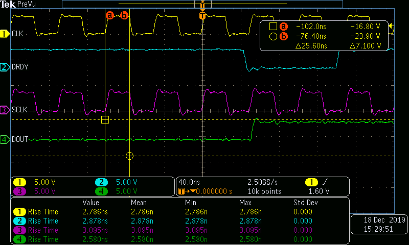
Also when i probe at SCLK or DOUT line the ADC data seems to be ok.

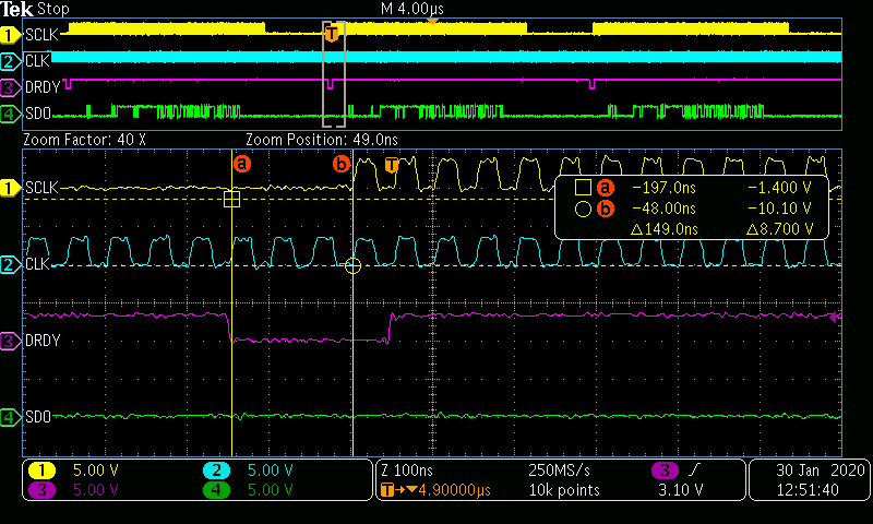
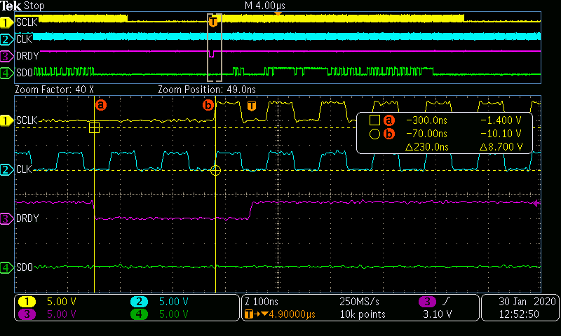
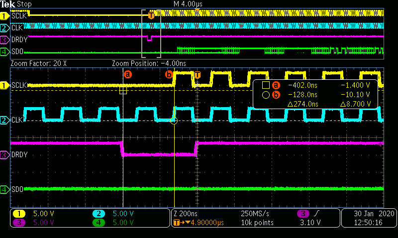
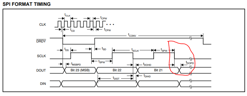
Probe Capacitance helps shape the Timing delay in the SPI Timing characteristics.

I had built 9 boards and found 5 boards work seamlessly at 20 MHz and all the board work at 5 MHz.

Need to understand what would be the optimal solution to have in the design to have consistent performance.

????? current design have only series termination and no provision for RC ,suggest what can be done to improve-wise the design ??????

Reducing the ripple in the SCLK also solves the issue by having the LOW pass RC in series.

SCLK scopeshoot:

Current configuration is SPI and TDM mode in ADS1278 using 7 channels active.

Appreciate your help in solving this issue.

Thanks,

Mani 

  • Hello Mani,

    What you are describing is a signal integrity issue on the digital lines.

    Some things you can try:

    1.  Can your host MCU or FPGA adjust the IO drive strength?  This will slow the edges down and typically reduces the ringing.

    2.  The ADS1278 launches data on the falling edge but holds the previous value for 10nS minimum.  Most systems capture on the rising edge, but if you capture SDO on the falling edge, this will give more time for settling.

    3.  You could try adding more delay between /DRDY falling and the first SCLK capture edge.  This will give more time for settling on the MSB.

    The only other options would be to improve your board layout or add additional RC filters on the SCLK and SDO lines, both of which will require a board change.

    If you can send a waveform capture of the /DRDY, SCLK, and SDO lines, I will take a look at it to see if there are any timing violations.

    Regards,
    Keith Nicholas
    Precision ADC Applications.

  • Thanks Keith Nicholas for your response.

    Timing capture:

    But the moment i probe the SDO or SCLK the issue gets resolved.

    We are looking for Software fix at this moment and take up layout change later in future releases.

    I could see the SPI FORMAT TIMING SPECIFICATION is met always when i probe communication lines.

    Thank you,

    Mani Kandan 

  • Hi Mani,

    There is a requirement for a 1 Fclk delay after the falling edge of /DRDY and before the first rising edge of SCLK.  In the case of CLK=20MHz, you will need a 50nS delay.  Based on your above waveforms, it looks like you only have a 10nS delay.

    Since SCLK=CLK, I suggest you run the SPI bus in stop-clock mode, where the SCLK is idle between conversions.  You can then force a >50nS delay between /DRDY falling edge and SCLK rising edge.

    Please let me know if you can adjust the waveforms to meet this requirement and if this fixes the problem.

    Thanks!

    Keith

  • Thanks Kieth,

    I will ask my SW team to look into and just check if this solves issue.

    can you provide me some information on the Stop-clock mode in SPI Bus,i can provide heads up on this to the SW team.

    Thanks very much

    Regards,

    Mani

  • Hi Mani,

    For the Stop-clock, this just means that the SCLK does not run continuously.  

    Keep SCLK low until /DRDY falling edge, delay by at least 1 Fclk period, and then start SCLK to retrieve data out of the device.  After all conversion results have been clocked out of the ADC, keep SCLK low until the next falling edge of /DRDY.

    Regards,
    Keith

  • Thanks keith,

    SW changes might take some time to get the test build from the team.

    once done will update.

    thanks for your support keith.

    regards,

    mani

  • Hi Keith,

    Update on SW changes on Adding delay between the DRDY and SCLK:

    still not able to make ADS1278 work at 20MHZ/10MHz,it works at 5MHZ always

    below are the snapshots:

    1. CLK=20MHZ, Tds=150ns(3 Tclk)

    2. CLK=10MHz ,Tds=230ns(2.3Tclk)

    3. Fclk=5MHz  ,Tds=274ns(Tclk=1.24)

    As per timing sequence for SPI, Tds shall have minimum 1 Tclk and as we meet this requirement and see that still problem is persisting.

    also note: previous while probing the SCLK line at 20MHz the ADS1278 works fine,but now after implementing this delay it does not work while probing.

    Let me know,what is the solutions to this issue.

    Thanks and regards,

    Mani

  • Hi Mani,

    CLK, SCLK, and /DRDY look correct.  Also, it does appear that the ADC is sending data out on DOUT.

    Since many of your boards work, and the load from the scope probe initially helped, I suspect that the problem may be with setup and hold time violations on the data capture.

    The ADS1278 launches data on the falling edge of SCLK, but it may take up to 26nS for the DOUT data to become valid.  At 20MHz SCLK, 26nS is longer than 1/2 clock period.  If your MCU/FPGA is capturing data on the rising edge of clock, you could be misreading the data.  If there is additional delay in SCLK due to long board traces, or if level translators or digital isolators are used, this can further delay and cause reading errors.

    Please send a scope plot showing SCLK and DOUT measured at your MCU/FPGA.  Please also confirm that you are capturing data on the falling edge of SCLK, and not the rising edge.

    Regards,
    Keith

  • Hi,

    I have tried to see the timing for tDOPD:

    @20MHz Clock: approx. 18ns

    @5MHz clock: approx. 20ns

    The overall trace length is around 37mm between the FPGA and ADC.

    Maximum time for tDOPD is 26ns for TDM mode of operation and we are within the limit.

    I will check withe the SW team and provide an update on Monday.

    see below scope capture for the tDOPD @20MHz:

    let me know if you have any comments,or i missed any ?

    Thanks,

    Mani

  • Hi Mani,

    I think your above scope picture is for SCLK=5MHz.  However, as you noted, you measured between 18-20nS.  With 37mm between the FPGA and the ADC, this could add another 6nS round trip, depending on where you measured the above signals.

    At 20MHz SCLK, with the ADC launching data on the falling edge of SCLK, if the FPGA then captures the data on the next rising edge, you could be very close to the timing setup time limit.  In addition, the FPGA will likely have its own setup time requirement which further tightens the timing budget.

    As I had stated before, it 'looks' like the ADC outputs data correctly when SCLK=20MHz.  If possible, for one of the boards that do not work correctly at SCLK=20MHz, input a DC voltage on channel 1 that is about 1/2 of positive full scale.  Assuming VREF=2.5V, set the input voltage to 1.25V.  Then capture /DRDY, SCLK, and SDO for the first 24 SCLKs and verify the code is close to what is expected.

    1/2 positive full scale code = 0x400000h

    Regards,
    Keith

  • yes you are right i see the data is being rolled out after DRDY asserts low,but anyways i will have to wait for software implementation for SCLK falling edge.

    i do verified the data in scope by feeding voltage to CH1 and checked the 24 SCLK falling edge. 

    by the way, how can i reduce the propagation delay to keep with the timing specification?

    currently the delay is between 19 ns to 24 ns at ADC end.(which is close to 26 ns)

    Thank you,

    Mani

  • Hi Mani,

    The max spec of the device is 26nS, so you have to work around that time; there is no way to reduce it. 

    The other delays due to board routing, level shifting, etc., can be helped by using a separate IO pin on your FPGA for a SCLK capture.  We do this on many of the evaluation boards.  SCLK and the return-SCLK are routed together and connected at the ADC SCLK pin.  This helps to reduce any additional delays, but it does require a board layout change and an additional IO pin on your FPGA.

    One other option if you are not running in high-speed mode is to run SCLK at 1/2 the frequency of CLK.  

    Regards,
    Keith

  • Noted keith,

    after optimizing the read strategy to falling edge and slight delay between DRDY to SCLK, we can read the data at 10MHZ clock. (but at 20MHZ we are reading one more bit at MSB.)

    I think the timing between the DRDY and SCLK was crucial and Propagation delay between the devices is the next key elements.

    currently tDOPD is on or just within the specification.(will take these layout changes to improve the timing on Propagation delay).

    Appreciate your consistent support and i hope you will keep it up going forward.

    Thanks,

    Mani