


Dear sir,
Please help me to come out of this problem.
Now i am dealing with ADS1248 for reading temperature using RTD Sensor, i am using below attached code and ADS1248 driver header file.
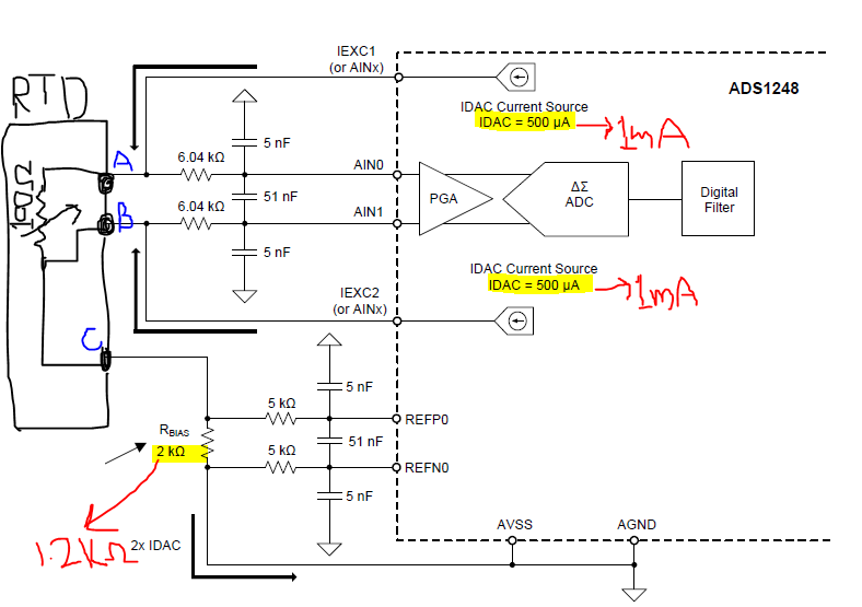
My SCHEMATIC Details:-
Schematic having below things:-
---------------------------------
AVDD = 5V (Proving input voltage of 5V through 10uF capacitor)
AVSS = GND
DVDD = 3.3V
DGND = GND
CURRNET SOURCES = IEXC1 and IEXC2
ANALOG INPUTS = AIN0 and AIN1
REFERENCE Resistor = 1.2kohm
I changed Rref to 1.2kohm because in ADS1248 Datasheet Vref should be below mid-SUPPLY of AVDD(Section 10.2.1.2.4).
Below voltages and currents with respective of ground i am getting:-
----------------------------------------------------------------------------------------
Before connecting RTD Sensor(three terminals(A,B,C) are open):-
At point 'A' voltage and current = 5.031v and 0.992mAmp
At point 'B' voltage and current = 5.030v and 0.993mAmp
At point 'C' voltage and current = 0v and 0mAmp
Voltage at Rref = 0.0v
After connecting RTD Sensor with 100ohms(means B and C terminals are shorted and Terminal A is open then connected RTD Sensor):-
At point 'A' voltage and current = 2.401v and 1.827mAmp
At point 'B' voltage and current = 2.398v and 1.827mAmp
At point 'C' voltage and current = 2.398v and 1.833mAmp
Voltage at Rref = 2.398v (Vref = AVDD/2==>5/2==>2.5v)
After setting all registers of ADS1248 like below code, then i am reading outputcode like below
output_code = ADS1248_RDATA();
but every time i am getting same value(output_code = 16777215) while changing RTD sensor manually like 100ohm to 150ohm. No change in output.
If change RTD sensor resistor value, it is not effecting at point A, B ,C means voltage not changing.
source code:-
--------------------------------------------------------------------------------------------------------------------------------------------------------------------------
main.c:-
-----------
  voltage_reference();
  Data_Rate();
  SetChannel();  //AIN0 FOR +VE(AINP) and AINP1 FOR -VE(AINN)
  SetGain();
  SetDRDYMode();
  SetIntRef();
  Test_write_IDAC0();
  Test_write_IDAC1_EXC1_EXC2();


 /*---------------------------------------------------------------------------------------------------------------*/
void voltage_reference(void)
{

	CHIPSELECT = 0;
	DelayMicroSeconds(1);

	  TXBSY |= 0;
	  SPI0DAT = ( ADS1248_CMD_WREG | ADS1248_2_MUX1); //0x42;
	  while(TXBSY);
	  TXBSY |= 0;


	  SPI0DAT = 0x01;
	  while(TXBSY);
	  TXBSY |= 0;


	  SPI0DAT = ADS1248_INT_REF0;  //0x20;   // Internal reference selected and internally connected to REFP0 and REFN0 input pins
	  while(TXBSY);
	  TXBSY |= 0;

	DelayMicroSeconds(1);
	CHIPSELECT = 1;

}
/*---------------------------------------------------------------------------------------------------------------*/
void Data_Rate(void)
{
	CHIPSELECT = 0;
	DelayMicroSeconds(1);

	  TXBSY |= 0;
	  SPI0DAT = ( ADS1248_CMD_WREG | ADS1248_3_SYS0);  //0x43;   //  //txdata;
	  while(TXBSY);
	  TXBSY |= 0;


	  SPI0DAT = 0x01;
	  while(TXBSY);
	  TXBSY |= 0;


	  SPI0DAT = ADS1248_DR_20;   //0x22;   //        gain = 4, datarate = 20sps
	  while(TXBSY);
	  TXBSY |= 0;

	DelayMicroSeconds(1);
	CHIPSELECT = 1;


}

/*---------------------------------------------------------------------------------------------------------------*/
void SetChannel(void)
{
	CHIPSELECT = 0;
	DelayMicroSeconds(1);

	  TXBSY |= 0;
	  SPI0DAT = ( ADS1248_CMD_WREG | ADS1248_0_MUX0); //0x40;   // //txdata;
	  while(TXBSY);
	  TXBSY |= 0;


	  SPI0DAT = 0x01;
	  while(TXBSY);
	  TXBSY |= 0;


	  SPI0DAT =  ADS1248_AINP0;   //0x01;   //    AIN0
	  while(TXBSY);
	  TXBSY |= 0;

	DelayMicroSeconds(1);
	CHIPSELECT = 1;

	DelayMicroSeconds(10000);

	CHIPSELECT = 0;
	DelayMicroSeconds(1);

	  TXBSY |= 0;
	  SPI0DAT =( ADS1248_CMD_WREG | ADS1248_0_MUX0);  //txdata;
	  while(TXBSY);
	  TXBSY |= 0;

	  SPI0DAT = 0x01;
	  while(TXBSY);
	  TXBSY |= 0;


	  SPI0DAT =  ADS1248_AINN1;   //AIN1
	  while(TXBSY);
	  TXBSY |= 0;

	DelayMicroSeconds(1);
	CHIPSELECT = 1;

}

/*---------------------------------------------------------------------------------------------------------------*/
void SetGain(void)
{
	CHIPSELECT = 0;
	DelayMicroSeconds(1);


	  TXBSY |= 0;
	  SPI0DAT =( ADS1248_CMD_WREG | ADS1248_3_SYS0); //txdata;
	  while(TXBSY);
	  TXBSY |= 0;


	  SPI0DAT = 0x01;
	  while(TXBSY);
	  TXBSY |= 0;


	  SPI0DAT =  ADS1248_GAIN_4;
	  while(TXBSY);
	  TXBSY |= 0;

	DelayMicroSeconds(1);
	CHIPSELECT = 1;

}

/*---------------------------------------------------------------------------------------------------------------*/
void SetDRDYMode(void)
{

	CHIPSELECT = 0;
	DelayMicroSeconds(1);

	  SPIEN     = 1;

	  TXBSY |= 0;
	  SPI0DAT = ( ADS1248_CMD_WREG | ADS1248_10_IDAC0);  //0x4A;   // //txdata;     IDAC REGISTER
	  while(TXBSY);
	  TXBSY |= 0;


	  SPI0DAT = 0x01;
	  while(TXBSY);
	  TXBSY |= 0;


	  SPI0DAT =  ADS1248_DRDY_OFF;  //0x06;   //  DRDY/OUT PIN ACT AS OUTPUT PIN AND 1000MICRO AMP CURRENT
	  while(TXBSY);
	  TXBSY |= 0;

	DelayMicroSeconds(1);
	CHIPSELECT = 1;


}
/*---------------------------------------------------------------------------------------------------------------*/
void SetIntRef(void)
{
	CHIPSELECT = 0;
	DelayMicroSeconds(1);


	  TXBSY |= 0;
	  SPI0DAT =( ADS1248_CMD_WREG | ADS1248_2_MUX1);//txdata;
	  while(TXBSY);
	  TXBSY |= 0;


	  SPI0DAT = 0x01;
	  while(TXBSY);
	  TXBSY |= 0;


	  SPI0DAT =  ADS1248_INT_VREF_ON;
	  while(TXBSY);
	  TXBSY |= 0;

	DelayMicroSeconds(1);
	CHIPSELECT = 1;

}

/*---------------------------------------------------------------------------------------------------------------*/

void Test_write_IDAC0(void)
{

	CHIPSELECT = 0;
	DelayMicroSeconds(1);


	  TXBSY |= 0;
	  SPI0DAT =( ADS1248_CMD_WREG | ADS1248_10_IDAC0);//txdata;
	  while(TXBSY);
	  TXBSY |= 0;


	  SPI0DAT = 0x01;
	  while(TXBSY);
	  TXBSY |= 0;


	  SPI0DAT =  ADS1248_IDAC_1000;
	  while(TXBSY);
	  TXBSY |= 0;

	DelayMicroSeconds(1);
	CHIPSELECT = 1;

}
/*---------------------------------------------------------------------------------------------------------------*/
void Test_write_IDAC1_EXC1(void)
{

		CHIPSELECT = 0;
	DelayMicroSeconds(1);


	  TXBSY |= 0;
	  SPI0DAT =( ADS1248_CMD_WREG | ADS1248_11_IDAC1);//txdata;
	  while(TXBSY);
	  TXBSY |= 0;


	  SPI0DAT = 0x01;
	  while(TXBSY);
	  TXBSY |= 0;


	  SPI0DAT =  ADS1248_IDAC1_EXT1;
	  while(TXBSY);
	  TXBSY |= 0;

	DelayMicroSeconds(1);
	CHIPSELECT = 1;


}

/*---------------------------------------------------------------------------------------------------------------*/
void Test_write_IDAC1_EXC2(void)
{

	CHIPSELECT = 0;
	DelayMicroSeconds(1);


	  TXBSY |= 0;
	  SPI0DAT =( ADS1248_CMD_WREG | ADS1248_11_IDAC1);//txdata;
	  while(TXBSY);
	  TXBSY |= 0;


	  SPI0DAT = 0x01;
	  while(TXBSY);
	  TXBSY |= 0;


	  SPI0DAT = ADS1248_IDAC1_EXT2;
	  while(TXBSY);
	  TXBSY |= 0;

	DelayMicroSeconds(1);
	CHIPSELECT = 1;


}
/*---------------------------------------------------------------------------------------------------------------*/


void ADS1248_Reset(void)
{

	CHIPSELECT = 0;
	DelayMicroSeconds(1);

	TXBSY |= 0;
	SPI0DAT = ADS1248_CMD_RESET;
	while(TXBSY);
	TXBSY |= 0;

	DelayMicroSeconds(1);
	CHIPSELECT = 1;

//  RESET_PIN =0;
//	DelayMicroSeconds(1);
//	RESET_PIN = 1;
//  DelayMicroSeconds(1);

}
/*-------------------------------------------------------------------------------------------------------------*/
void Test_write_IDAC1_EXC1_EXC2(void)
{


  CHIPSELECT = 0;
	DelayMicroSeconds(1);

	  TXBSY |= 0;
	  SPI0DAT = 0x4B;  //( ADS1248_CMD_WREG | ADS1248_11_IDAC1);
	  while(TXBSY);
	  TXBSY |= 0;


	  SPI0DAT = 0x01;
	  while(TXBSY);
	  TXBSY |= 0;


	  SPI0DAT = 0x89;    //0x89 for EXC1 and EXC2   and   0x32 for AIN3 and AIN2
	  while(TXBSY);
	  TXBSY |= 0;

	DelayMicroSeconds(1);
	CHIPSELECT = 1;
}


/*--------------------------------------------------------------------------------*/
void Interrupts_Init(void)
{
  EA = 1;     // Enable global interrupts
  EIE1 |= 0x01; //Enable Serial Peripheral Interface (SPI0) Interrupt.Enable Interrupt requests generated by the SPIF flag (SPI0CN.7)
  // EIP1 |= 0x01; //SPI0 interruptS set to high priority level
  EX0 = 1;  //External interrrupt0 enabled
  IT0 = 1;  //INT0 is falling edge triggered
	PX0 = 1;   //INT0 is High PRIORITY

}

/*----------------------------------------------------------------------------------*/
void ADS1248_SYNC(void)
{

  CHIPSELECT = 0;
	DelayMicroSeconds(1);

	  TXBSY |= 0;
	  SPI0DAT = ADS1248_CMD_SYNC;
	  while(TXBSY);
	  TXBSY |= 0;

	DelayMicroSeconds(1);
	CHIPSELECT = 1;
}

/*----------------------------------------------------------------------------------*/
void ADS1248_SDATAC(void)
{

  CHIPSELECT = 0;
	DelayMicroSeconds(1);

	  TXBSY |= 0;
	  SPI0DAT = ADS1248_CMD_SDATAC;
	  while(TXBSY);
	  TXBSY |= 0;

	DelayMicroSeconds(1);
	CHIPSELECT = 1;
}

/*-----------------------------------------------------------------------------------------------*/
unsigned char ADS1248ReceiveByte(void)
{
	unsigned char Result = 0;
	while(TXBSY);			                           // Make sure nothing is already in the TX buffer
	TXBSY |= 0;
	SPI0DAT = 0xFF;		                           // Send out NOP to initiate SCLK
	while(TXBSY);			                           // Wait until all data is transmitted (received)
	TXBSY |= 0;
	Result = SPI0DAT;					                   // Capture the receive buffer and return the Result
	return Result;
}

/*-------------------------------------------------------------------------------------------------------*/
unsigned char ADS1248_RREG(void)
{
  CHIPSELECT = 0;
	//DelayMicroSeconds(1);

	  TXBSY |= 0;
	  SPI0DAT =( ADS1248_CMD_RREG | ADS1248_10_IDAC0);//txdata;
	  while(TXBSY);
	  TXBSY |= 0;


	  SPI0DAT = 0x01;
	  while(TXBSY);
	  TXBSY |= 0;


	  SPI0DAT =  0xFF;
	  while(TXBSY);
	  TXBSY |= 0;

	//DelayMicroSeconds(1);
	CHIPSELECT = 1;

 return SPI0DAT;
}
/*----------------------------------------------------------------------------------------------*/

unsigned long int ADS1248_RDATA(void)
{


 unsigned char var;
 unsigned long int result;
 char res[3];

 CHIPSELECT = 0;
	Delayms(1);   //DelayMicroSeconds(1);

 var = SPI0_Write(ADS1248_CMD_RDATA);    //Read data once
 res[0] = ADS1248ReceiveByte();
 res[1] = ADS1248ReceiveByte();
 res[2] = ADS1248ReceiveByte();
 var = ADS1248ReceiveByte();         //a NOP can be sent to force DOUT/DRDY high if no other command is pending

  Delayms(1); // DelayMicroSeconds(1);
	CHIPSELECT = 1;


 result = 0x00;
 result = (res[0] & 0xFF);    //must & 0xFF otherwise random errors occure
 result = (result << 8);
 result = result | ( res[1] & 0xFF );
 result = (result << 8);
 result = result | ( res[2] & 0xFF );

 return( result );
}

-------------------------------------------------------------------------------------------------------------------------------------------------------------------------------------
ads1248.h:-
---------------
#ifndef __ADS1248_H
#define __ADS1248_H
//#define USE_INTER_VREF
/* Error Return Values */
#define ADS1248_NO_ERROR 0
#define ADS1248_ERROR -1
/* Command Definitions */
// System Control
#define ADS1248_CMD_WAKEUP 0x00
#define ADS1248_CMD_SLEEP 0x03
#define ADS1248_CMD_SYNC 0x05
#define ADS1248_CMD_RESET 0x07
#define ADS1248_CMD_NOP 0xFF
// Data Read
#define ADS1248_CMD_RDATA 0x13
#define ADS1248_CMD_RDATAC 0x15
#define ADS1248_CMD_SDATAC 0x17
// Read Register
#define ADS1248_CMD_RREG 0x20
// Write Register
#define ADS1248_CMD_WREG 0x40
// Calibration
#define ADS1248_CMD_SYSOCAL 0x60
#define ADS1248_CMD_SYSGCAL 0x61
#define ADS1248_CMD_SELFOCAL 0x62
/* ADS1248 Register Definitions */
#define ADS1248_0_MUX0 0x00
#define ADS1248_1_VBIAS 0x01
#define ADS1248_2_MUX1 0x02
#define ADS1248_3_SYS0 0x03
#define ADS1248_4_OFC0 0x04
#define ADS1248_5_OFC1 0x05
#define ADS1248_6_OFC2 0x06
#define ADS1248_7_FSC0 0x07
#define ADS1248_8_FSC1 0x08
#define ADS1248_9_FSC2 0x09
#define ADS1248_10_IDAC0 0x0A
#define ADS1248_11_IDAC1 0x0B
#define ADS1248_12_GPIOCFG 0x0C
#define ADS1248_13_GPIODIR 0x0D
#define ADS1248_14_GPIODAT 0x0E
/* ADS1248 Register 0 (MUX0) Definition */
// Bit 7 | Bit 6 | Bit 5 | Bit 4 | Bit 3 | Bit 2 | Bit 1 | Bit 0
//--------------------------------------------------------------------------------------------
// BCS[1:0] | MUX_SP[2:0] | MUX_SN[2:0]
//
// Define BCS (burnout current source)
#define ADS1248_BCS_OFF 0x00
#define ADS1248_BCS_500nA 0x40
#define ADS1248_BCS_2uA 0x80
#define ADS1248_BCS_10uA 0xC0
// Define Positive MUX Input Channels
#define ADS1248_AINP0 0x00
#define ADS1248_AINP1 0x08
#define ADS1248_AINP2 0x10
#define ADS1248_AINP3 0x18
#define ADS1248_AINP4 0x20
#define ADS1248_AINP5 0x28
#define ADS1248_AINP6 0x30
#define ADS1248_AINP7 0x38
// Define Negative Mux Input Channels
#define ADS1248_AINN0 0x00
#define ADS1248_AINN1 0x01
#define ADS1248_AINN2 0x02
#define ADS1248_AINN3 0x03
#define ADS1248_AINN4 0x04
#define ADS1248_AINN5 0x05
#define ADS1248_AINN6 0x06
#define ADS1248_AINN7 0x07
/* ADS1248 Register 1 (VBIAS) Definition */
// Bit 7 | Bit 6 | Bit 5 | Bit 4 | Bit 3 | Bit 2 | Bit 1 | Bit 0
//--------------------------------------------------------------------------------------------
// VBIAS[7:0]
//
#define ADS1248_VBIAS_OFF 0x00
#define ADS1248_VBIAS0 0x01
#define ADS1248_VBIAS1 0x02
#define ADS1248_VBIAS2 0x04
#define ADS1248_VBIAS3 0x08
#define ADS1248_VBIAS4 0x10
#define ADS1248_VBIAS5 0x20
#define ADS1248_VBIAS6 0x40
#define ADS1248_VBIAS7 0x80
/* ADS1248 Register 2 (MUX1) Definition */
// Bit 7 | Bit 6 | Bit 5 | Bit 4 | Bit 3 | Bit 2 | Bit 1 | Bit 0
//--------------------------------------------------------------------------------------------
// CLKSTAT | VREFCON[1:0] | REFSELT[1:0] | MUXCAL[2:0]
//
// Define Internal Reference
#define ADS1248_INT_VREF_OFF 0x00
#define ADS1248_INT_VREF_ON 0x20
#define ADS1248_INT_VREF_CONV 0x40
// Define Reference Select
#define ADS1248_REF0 0x00
#define ADS1248_REF1 0x08
#define ADS1248_INT 0x10
#define ADS1248_INT_REF0 0x18
// Define System Monitor
#define ADS1248_MEAS_NORM 0x00
#define ADS1248_MEAS_OFFSET 0x01
#define ADS1248_MEAS_GAIN 0x02
#define ADS1248_MEAS_TEMP 0x03
#define ADS1248_MEAS_REF1 0x04
#define ADS1248_MEAS_REF0 0x05
#define ADS1248_MEAS_AVDD 0x06
#define ADS1248_MEAS_DVDD 0x07
/* ADS1248 Register 3 (SYS0) Definition */
// Bit 7 | Bit 6 | Bit 5 | Bit 4 | Bit 3 | Bit 2 | Bit 1 | Bit 0
//--------------------------------------------------------------------------------------------
// 0 | PGA[2:0] | DOR[3:0]
//
// Define Gain
#define ADS1248_GAIN_1 0x00
#define ADS1248_GAIN_2 0x10
#define ADS1248_GAIN_4 0x20
#define ADS1248_GAIN_8 0x30
#define ADS1248_GAIN_16 0x40
#define ADS1248_GAIN_32 0x50
#define ADS1248_GAIN_64 0x60
#define ADS1248_GAIN_128 0x70
//Define data rate
#define ADS1248_DR_5 0x00
#define ADS1248_DR_10 0x01
#define ADS1248_DR_20 0x02
#define ADS1248_DR_40 0x03
#define ADS1248_DR_80 0x04
#define ADS1248_DR_160 0x05
#define ADS1248_DR_320 0x06
#define ADS1248_DR_640 0x07
#define ADS1248_DR_1000 0x08
#define ADS1248_DR_2000 0x09
/* ADS1248 Register 4 (OFC0) Definition */
// Bit 7 | Bit 6 | Bit 5 | Bit 4 | Bit 3 | Bit 2 | Bit 1 | Bit 0
//--------------------------------------------------------------------------------------------
// OFC0[7:0]
//
/* ADS1248 Register 5 (OFC1) Definition */
// Bit 7 | Bit 6 | Bit 5 | Bit 4 | Bit 3 | Bit 2 | Bit 1 | Bit 0
//--------------------------------------------------------------------------------------------
// OFC1[7:0]
//
/* ADS1248 Register 6 (OFC2) Definition */
// Bit 7 | Bit 6 | Bit 5 | Bit 4 | Bit 3 | Bit 2 | Bit 1 | Bit 0
//--------------------------------------------------------------------------------------------
// OFC2[7:0]
//
/* ADS1248 Register 7 (FSC0) Definition */
// Bit 7 | Bit 6 | Bit 5 | Bit 4 | Bit 3 | Bit 2 | Bit 1 | Bit 0
//--------------------------------------------------------------------------------------------
// FSC0[7:0]
//
/* ADS1248 Register 8 (FSC1) Definition */
// Bit 7 | Bit 6 | Bit 5 | Bit 4 | Bit 3 | Bit 2 | Bit 1 | Bit 0
//--------------------------------------------------------------------------------------------
// FSC1[7:0]
//
/* ADS1248 Register 9 (FSC2) Definition */
// Bit 7 | Bit 6 | Bit 5 | Bit 4 | Bit 3 | Bit 2 | Bit 1 | Bit 0
//--------------------------------------------------------------------------------------------
// FSC2[7:0]
//
/* ADS1248 Register A (IDAC0) Definition */
// Bit 7 | Bit 6 | Bit 5 | Bit 4 | Bit 3 | Bit 2 | Bit 1 | Bit 0
//--------------------------------------------------------------------------------------------
// ID[3:0] | DRDY_MODE | IMAG[2:0]
//
// Define DRDY mode on DOUT
#define ADS1248_DRDY_OFF 0x00
#define ADS1248_DRDY_ON 0x08
//Define IDAC Magnitude
#define ADS1248_IDAC_OFF 0x00
#define ADS1248_IDAC_50 0x01
#define ADS1248_IDAC_100 0x02
#define ADS1248_IDAC_250 0x03
#define ADS1248_IDAC_500 0x04
#define ADS1248_IDAC_750 0x05
#define ADS1248_IDAC_1000 0x06
#define ADS1248_IDAC_1500 0x07
/* ADS1248 Register B (IDAC1) Definition */
// Bit 7 | Bit 6 | Bit 5 | Bit 4 | Bit 3 | Bit 2 | Bit 1 | Bit 0
//--------------------------------------------------------------------------------------------
// I1DIR[3:0] | I2DIR[3:0]
//
// Define IDAC1 Output
#define ADS1248_IDAC1_A0 0x00
#define ADS1248_IDAC1_A1 0x10
#define ADS1248_IDAC1_A2 0x20
#define ADS1248_IDAC1_A3 0x30
#define ADS1248_IDAC1_A4 0x40
#define ADS1248_IDAC1_A5 0x50
#define ADS1248_IDAC1_A6 0x60
#define ADS1248_IDAC1_A7 0x70
#define ADS1248_IDAC1_EXT1 0x80
#define ADS1248_IDAC1_EXT2 0x90
#define ADS1248_IDAC1_OFF 0xF0
// Define IDAC2 Output
#define ADS1248_IDAC2_A0 0x00
#define ADS1248_IDAC2_A1 0x01
#define ADS1248_IDAC2_A2 0x02
#define ADS1248_IDAC2_A3 0x03
#define ADS1248_IDAC2_A4 0x04
#define ADS1248_IDAC2_A5 0x05
#define ADS1248_IDAC2_A6 0x06
#define ADS1248_IDAC2_A7 0x07
#define ADS1248_IDAC2_EXT1 0x08
#define ADS1248_IDAC2_EXT2 0x09
#define ADS1248_IDAC2_OFF 0x0F
/* ADS1248 Register C (GPIOCFG) Definition */
// Bit 7 | Bit 6 | Bit 5 | Bit 4 | Bit 3 | Bit 2 | Bit 1 | Bit 0
//--------------------------------------------------------------------------------------------
// IOCFG[7:0]
//
// Define GPIO (0-Analog; 1-GPIO)
#define ADS1248_GPIO_0 0x01
#define ADS1248_GPIO_1 0x02
#define ADS1248_GPIO_2 0x04
#define ADS1248_GPIO_3 0x08
#define ADS1248_GPIO_4 0x10
#define ADS1248_GPIO_5 0x20
#define ADS1248_GPIO_6 0x40
#define ADS1248_GPIO_7 0x80
/* ADS1248 Register D (GPIODIR) Definition */
// Bit 7 | Bit 6 | Bit 5 | Bit 4 | Bit 3 | Bit 2 | Bit 1 | Bit 0
//--------------------------------------------------------------------------------------------
// IODIR[7:0]
//
// Define GPIO Direction (0-Output; 1-Input)
#define ADS1248_IO_0 0x01
#define ADS1248_IO_1 0x02
#define ADS1248_IO_2 0x04
#define ADS1248_IO_3 0x08
#define ADS1248_IO_4 0x10
#define ADS1248_IO_5 0x20
#define ADS1248_IO_6 0x40
#define ADS1248_IO_7 0x80
/* ADS1248 Register E (GPIODAT) Definition */
// Bit 7 | Bit 6 | Bit 5 | Bit 4 | Bit 3 | Bit 2 | Bit 1 | Bit 0
//--------------------------------------------------------------------------------------------
// IOIDAT[7:0]
//
#define ADS1248_OUT_0 0x01
#define ADS1248_OUT_1 0x02
#define ADS1248_OUT_2 0x04
#define ADS1248_OUT_3 0x08
#define ADS1248_OUT_4 0x10
#define ADS1248_OUT_5 0x20
#define ADS1248_OUT_6 0x40
#define ADS1248_OUT_7 0x80
typedef unsigned char uint8_t;
typedef unsigned short uint16_t;
typedef unsigned int uint32_t;
void ADS1248_GPIO_Init(void);
void ADS1248_SPI_Init(void);
static unsigned char ADS1248_SPI_SendByte(unsigned char outByte);
int ADS1248WaitForDataReady(int Timeout);
void ADS1248ReadRegister(int StartAddress, int NumRegs, unsigned * pData); // Read the register(s) (NumReg is the total number of registers read)
void ADS1248WriteRegister(int StartAddress, int NumReg, unsigned * pData); // Write the register(s) (NumReg is the total number of registers written)
//void ADS1248WriteSequence(int StartAddress, int NumReg, unsigned * pData); // Write the register(s) (NumReg is the total number of registers written)
void ADS1248SendRDATAC(void); // Read data continuous mode
void ADS1248SendSDATAC(void); // Stop read data continuous mode
void ADS1248SendSYSOCAL(void); // System offset calibration
void ADS1248SendSYSGCAL(void); // System gain calibration
void ADS1248SendSELFOCAL(void); // Self offset calibration
/* Register Set Value Commands */
// Relate to MUX0
int ADS1248SetBurnOutSource(int BurnOut);
int ADS1248SetChannel(int pMux, int vMux); // pMux (0=AINP. 1=AINN); vMux (value of mux channel selection)
// Relate to VBIAS
int ADS1248SetBias(unsigned char vBias);
// Relate to MUX1
int ADS1248SetIntRef(int sRef);
int ADS1248SetVoltageReference(int VoltageRef);
int ADS1248SetSystemMonitor(int Monitor);
// Relate to SYS0
int ADS1248SetGain(int Gain);
int ADS1248SetDataRate(int DataRate);
// Relate to OFC (3 registers)
int ADS1248SetOFC(long RegOffset);
// Relate to FSC (3 registers)
int ADS1248SetFSC(long RegGain);
// Relate to IDAC0
int ADS1248SetDRDYMode(int DRDYMode);
int ADS1248SetCurrentDACOutput(int CurrentOutput);
// Relate to IDAC1
int ADS1248SetIDACRouting(int IDACroute, int IDACdir); // IDACRoute (0 = I1DIR, 1 = I2DIR)
// Relate to GPIOCFG
int ADS1248SetGPIOConfig(unsigned char cdata);
// Relate to GPIODIR
int ADS1248SetGPIODir(unsigned char cdata);
// Relate to GPIODAT
int ADS1248SetGPIO(unsigned char cdata);
/* Register Get Value Commands */
// Relate to MUX0
int ADS1248GetBurnOutSource(void);
int ADS1248GetChannel(int cMux);
// Relate to VBIAS
unsigned char ADS1248GetBias(void);
//Relate to MUX1
int ADS1248GetCLKSTAT(void);
int ADS1248GetIntRef(void);
int ADS1248GetVoltageReference(void);
int ADS1248GetSystemMonitor(void);
// Relate to SYS0
int ADS1248GetGain(void);
int ADS1248GetDataRate(void);
// Relate to OFC (3 registers)
long ADS1248GetOFC(void);
// Relate to FSC (3 registers)
long ADS1248GetFSC(void);
// Relate to IDAC0
//int ADS1248GetID(void);
int ADS1248GetDRDYMode(void);
int ADS1248GetCurrentDACOutput(void);
// Relate to IDAC1
int ADS1248GetIDACRouting(int WhichOne); // IDACRoute (0 = I1DIR, 1 = I2DIR)
// Relate to GPIOCFG
unsigned char ADS1248GetGPIOConfig(void);
// Relate to GPIODIR
unsigned char ADS1248GetGPIODir(void);
// Relate to GPIODAT
unsigned char ADS1248GetGPIO(void);
/* Miscellaneous Commands */
int ADS1248RDATACRead(void); // reads data directly based on RDATAC mode (writes NOP) and 32 SCLKs
int ADS1248RDATARead(void);
void Delay1us(void);
void Delay10us(void);
void Delay200us(void);
void Delay10ms(void);
void Delay20ms(void);
void ADS1248SendSYSNC(void);
void ADS1248SendRDATA(void);
void ADS1248_Reset(void);
unsigned char Ads_Calibrate(unsigned int Gain);
#endif
Schematic:-
-------------------------
So please see my problem give me suggestion i red ADS1248 Datasheet, Basic RTD sensor using datasheet, i got formulas for converting outputcode into resistor and then resistor to temperature.
1) Internally how ADS1248 convert analog data to digital form?
2) Is it compulsory to calibrate digital data to get correct output code?
Please help me. I am struggling so much since one month.
Thanks in advance,
Regards,
amarr

