This thread has been locked.

If you have a related question, please click the "Ask a related question" button in the top right corner. The newly created question will be automatically linked to this question.

ADS122U04: channel crosstalk/charge-injection

Part Number: ADS122U04
Other Parts Discussed in Thread: ADS124S08

Hi TI Team,

I have some questions about the ADS122u04.

I am using this IC in a unipolar configuration. The analog supply voltage is 5.3V (±1%), the digital supply is at 3.3V (±1%). All analog input signals are single ended referenced to AVSS.
The ADC is configured in turbo mode, and single-shot conversion mode. The internal multiplexer manually scans over each channel. After one sample is taken the multiplexer switches to the next channel.
To make use of the whole absolute input voltage range of the analog inputs, I disabled the PGA and use only gains of 1, 2 and 4.
Configuration:

The analog voltage on the inputs ranges from 1mV to 5,002V in my application. I use a RC filter with 1kOhm and 100nF at the input.

According to the datasheet the absolute input current of the analog inputs is ±10nA with disabled PGA in turbo mode. This causes a voltage drop of ±10µV across the filter resistor.

Unfortunately this isn´t the case in my application. I observed a drop voltage across this resistor which is dependent on the voltage level of the pin that was sampled in the previous cycle. At this point I´m inclined to think that there is a substantial amount of charge injection / crosstalk through the multiplexer. I couldn´t find any information on multiplexer timing / charge injection in the datasheet though.

To further verify this thesis I replaced the 1kOhm resistor with a 0 Ohm jumper, and fed the ADC input with an opamp output directly. The ADC now measures the predicted voltage. A low impedance driving source seems to get rid of the problem for the most part.

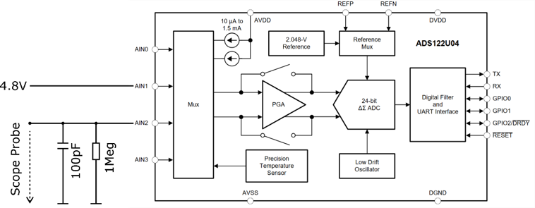
I´ve set up a circuit to verify the multiplexer function as follows:

I´ve connected a DC voltage source to the AIN1 pin of the device. AIN2 is loaded with a 1Meg resistor to ground, parallel to a 100pF capacitor. I´ve connected a 1:1 scope probe from AIN2 to ground. The probe loads the Input with additional 14pF and 1Meg to ground. Once the multiplexer starts switching the scope shows very large spikes on AIN2. The amplitude of the spikes are dependent on the DC level on pin AIN1.

What causes this problem? What is the recommended workaround except a low impedance driving source? Is this effect dependent on the device temperature as well?

Upon research in this forum I found a post from Ben Benjamin discussing the dynamic range of this ADC.

e2e.ti.com/.../793376

He says that, quote: “Another consideration is the ADS122U04 is considered a DC type sensor device in that its primary purpose is to measure signals near DC levels.”

I use an auto-calibrate function in my application, which switches between the signal of interest, and a known reference source. This results in a ~105Hz square wave signal on the ADC input. The voltage in this case can swing from 0,614V to 4,8V. Is this still considered DC level? I couldn´t find any information about the analog frontend bandwidth in the datasheet, only information on the digital filter bandwidth. Is the internal frontend circuitry fast enough to give me precise readings in the application described above?

The datasheets states the following about the digital filter:

“The device uses a linear-phase finite impulse response (FIR) digital filter that performs both filtering and decimation of the digital data stream coming from the modulator”

Does the digital filter receive any channel information, or does it filter the products of multiple MUXed channels?

Thank you in advance!

Best regards

Lukas

  • Unfortunately there are some pictures missing in my post above.

    I´ve attached them here.

    ADC configuration:

    Circuit to verify the multiplexer function:

    The spikes on pin AIN2:

  • Hi Lukas,

    Welcome to the E2E forum!  In your initial testing you were seeing a combination of charge injection and analog settling.  In many applications the PGA will be enabled which adds a high-impedance input to the source.  However, with single-ended measurements the PGA must be bypassed.  The input now becomes a switched capacitor input and the capacitor value changes as you increase gain.  This means that the input capacitor value changes with gain applied.

    There is a pre-charge buffer circuit which helps limit the effect of the movement of charge at the input, but it will not eliminate it.  Using Turbo mode worsens the effect as the sampling by the modulator is twice that of Normal mode.  Having an RC filter at the front will add an additional analog settling delay as it will take some time for the pathway to settle.  Once settled you would see something more like the typical response graphs shown in the ADS122U04 datasheet as far as average current.  I would suspect that the current would be slightly higher using voltages greater than 3.3V for the analog while using Turbo mode, but I don't have specific data to verify that hypothesis.

    The mux is break before make, but because the input is switched cap the charge already on the input capacitors will take some amount of time before it equalizes.  As to the modulator/digital filter, the input of the device is oversampled (512kHz in Turbo mode) and converted to a Delta-Sigma modulator bit stream.  This D-S modulator basically takes the quantization noise and pushes it to the higher frequencies.  The digital filter takes the modulator bit stream and passes the data through a low-pass filter.  The digital filter is reset at the start of the conversion when the mux is switched.  However, any residual charge on the input caps will be a part of the next conversion until analog settling is complete.

    Bandwidth for 2ksps is shown on page 26 in the last graph in Figure 56.  You will notice that even though the modulator sampling is taking place at 512kHz, the low-pass filter response is somewhat SINC like in nature where the roll-off has a bouncing ball effect.  In Table 12 there is the -3dB bandwidth for the various device data rates.  At 2ksps Turbo mode the cut-off frequency is typically 967.6Hz.  105Hz would be well within this region so it should be measurable.  However, due to the settling nature in PGA bypass mode, the input square wave may appear to be something a bit different when the output conversion data are plotted.

    Some of our later devices, such as the ADS124S08, have a built-in programmable delay which adds some time following the mux switch to the start of the conversion period.  The ADS122U04 unfortunately does not have this feature.  Possible workarounds would be to discard a sample(s) following a mux change.  Another option would be to switch the mux, then have the micro wait a predetermined amount of time and then send the START/SYNC command to restart the conversion.  You could also play with the input filter values to shorten analog settling and still have an adequate anti-aliasing filter.

    Best regards,

    Bob B