This thread has been locked.

If you have a related question, please click the "Ask a related question" button in the top right corner. The newly created question will be automatically linked to this question.

ADC12DJ5200RF: Data misalignment between DA and DB lanes

Part Number: ADC12DJ5200RF

I am designing a board with the ADC12DJ5200RF.

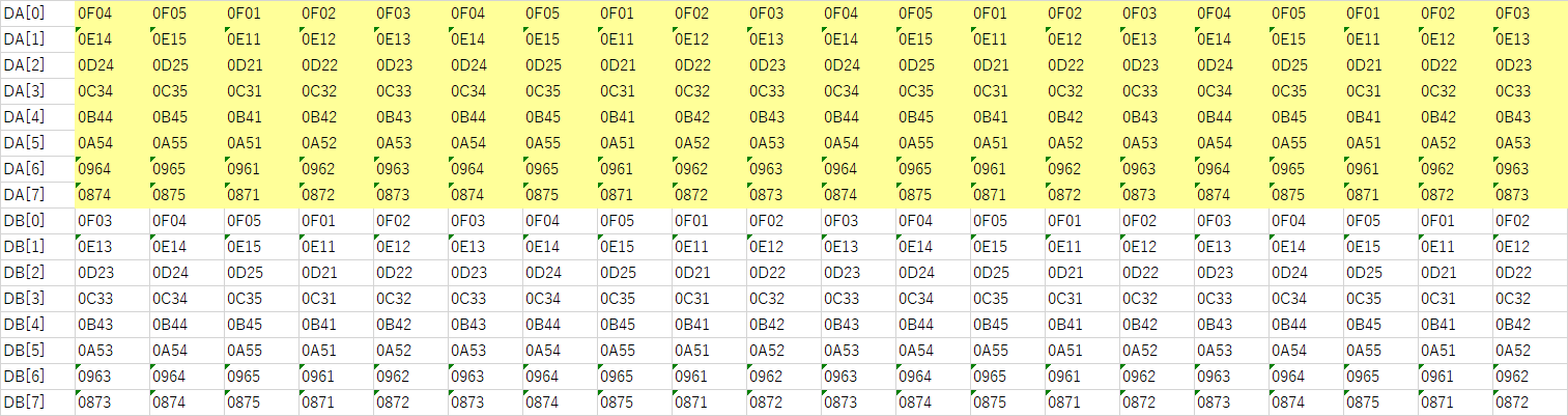
When I sent test data from the ADC to the FPGA using JMODE1, I noticed that the data sometimes deviated between 8 lanes of the DA and 8 lanes of the DB.

 (If the FPGA receives the data correctly, I think DA [x] = DB [x], but it doesn't.)

Will it be solved by setting something on the FPGA side or by setting something on the ADC side?

  • Hi,

    I apologize for the delay. I will look into these settings and get back with you shortly..

    Regards,

    Rob

  • Hi,

    This seems to be a lane release issue. If this occurs ‘sometimes’, so a fixed SW correction probably won't work.

    Is the mismatch always by one sample or can it be more/variable?

    Regards,

    Rob

  • Hi,

    This event seems to happen about 40% of the time.

    It is not yet possible to determine whether it is a problem of how to implement the JESDIP peripheral circuit on the FPGA side or a problem of ADC configuration.

  • Hi,

    Here are a few more things to try:

    • The 5200RF implements the 16 lanes as two links with 8 lanes each. Is the FPGA receiver IP set up as one link with 16 lanes or two of 8?
    • Try a ramp test mode and capture data (into an ILA) as soon as the lanes are released. All 16 lanes should release together and show a ramp. In addition, they should all have the same data on each cycle.
    • If the top 8 lanes are aligned among each other, but skewed with respect to the bottom 8 lanes (which are also aligned within themselves), then see next steps
      • Ensure that the SYSREF windowing is set up correctly in the ADC. This is a guess, because I don’t know exactly how SYSREF is implemented for aligning the frames inside the device, but it could offer some inputs
      • Use the slowest sampling clock possible and generate a SYSREF that will meet the setup and hold times with respect to the clock, see if this eliminates the mismatch.
      • Also check the logic generating the SYSREF into the FPGA IP (for timing)

    Regards,

    Rob