This thread has been locked.

If you have a related question, please click the "Ask a related question" button in the top right corner. The newly created question will be automatically linked to this question.

ADS1232 unwanted internal offset

Other Parts Discussed in Thread: ADS1232

Hi,

I have a problem using ads1232,

only SCLK , DOUT/DRDY connected through  series FerriteBead(200_ohm@100MHZ) to Micro,( two 27pf caps from those pins to GND are added in ads1232 side as low pass filter for UHF and GHZ noises )

the /PDWN  is connected to external reset circuitry that have voltage between 4.0 to 5.0 volts,( one 1k series resistor and 27pf cap exist here as LowPass filter )

it has a 500ms delay after powering up the digital and analog sections  (pulls down the /PDWN pin) thus it is enough for initial reset of ads1232 !

the gain is set to 128 , speed for 10SPS , TEMP = 0  , A0 = 0 , AVDD = 5.0 , DVDD = 5.0 from different REGs ,   AGND , DGND are connected in one point near the main CAP of POWER ;

it works fine in the most of times, it has peak to peak noise in my system ( +- 30 ) nearly twice the ti_pdf mentioned, and I have stable readong of 60/8,000,000 = 133,000 counts , this is enough for my system.


the problem is here:

some times after powerup or in normal operation , the reading of a2d if shifted by -8500 ( eg: from 139,500 it jumps down to 131,000 )

( or from 310,000 it jumps down to 301,500 )

but the  gain is satble..

and this unwanted huge offset will remain until :

1. turn off then turn on the system , sometimes removes the offset

2. manually pulling down the /PDWN to gnd by a wire! ( every time this will remove the offset temporarily , but the problem may occure some minutes later!)

3. using the 26 clock for internal offset calibration,( every time this will remove the offset temporarily , but the problem may occure some minutes later!)


because of unpredictable occurance of this issue , the system is unreliable,

what is the source of this ( internal offset registers  UNcalibrator ) ???? 

what changes should I do for solving the problem?

Best regards,

notes on FerriteBead and cap

( I think  the 27pf cap connected to ads1232 pins are small enough to have no effects in loading and changing characteristics of ads1232 )

( the FerriteBead(150nH) and 27pf cap make 82MHz corner frequency for LowPass filter for reducing EMI noises from Digital cpu side to analog side )


  • MH,

    All delta-sigma parts have some inherit offset.  There may be some additional offset due to MUX and PGA.  This is easily subtracted out if you do the self offset cal (26 SCLKs.)  Basically this involves an internal short at the inputs which should produce a zero code.  Any difference is either added or subtracted out so that the actual output data is zero.

    What else can also affect the result?  You mentioned that you have noise that does not meet datasheet performance.  This is usually due to the reference or the grade and placement of the cap connected to pins 9 and 10 of the ADS1232.  Board layout may also be a consideration.  As noise can affect the results of the offset calibration, you really need to minimize the noise first.

    It is also a good idea to run the offset calibration periodically, especially when you change mux inputs, change PGA settings, or if there are changes in temperature around the device itself.

    Best regards,

    Bob B

  • Thanks Bob,

    your words are exactly correct,

    but the offset of -8500 counts equal to 13 bits of 24 bits a2d,( I think the offset errors of internal MUX and PGA in CMOS design may be large

    as 10mv in 2.500 v ( 3 bits in 11 bits    or   16bits in 24 bits a2d ) , so the amount of offset value is not my concern , but the unprogrammed and suddenly occurance is.

    and this suddenly appeared value in a2d readings is un controlled , un programmed and it behaves like an unknown noise , or hack!!!

    and I couldn't find the source of this unpredictable behavior of my design,

    in other hand , I can't rely on system , because after  running the offset calibration periodically , I don't know when that offset value will be appear again,

    thus my a2d readings will be unreliable.


    one point:

    -In 3 different pcb's I saw the same unregular, unpredictable , jumps in a2d readings, but the value of changes are nearly the same ( nearly -8500 counts )

    Best Regard

  • MH,

    I can tell you that this is not normal behaviour and you may want to take a look at what is common in the three PCBs you generated.  I can tell you that we have seen some problems when inductors are used on the supplies and ground.

    Before I can be of more help I need more specifics.  I need schematics.  What is the PGA setting?  What is your reference?  What kind of sensor are you using?  Is it possible that there is a supply glitch, or a glitch on the PWRDN pin?  Is it possible that the sensor is drifting outside of the common mode input range?

    One thing you can try is to simplify the circuit.  For  example, replace ferrites/inductors with 0 ohm resistors and remove caps.  If your problem goes away, you can target the areas where the parts were removed.  Also review the reference design as shown in the reference design user guide for the ADS1232.  I've attached the user guide to this post.

    Best regards,

    Bob B


    sbau120a.pdf
  • Hi Bob,

    The PGA is hard wired to 128 , 

    Reference and analog Supply is LM2940-5 , and has 100uF cap near its input and , 100uF+100nF caps in its output  to AGND,( AVDD = +5.0v )

    Sensor:350...450 Ohm  Loadcell ( Common mode is near 2.500v and is stable ) and signal : 0.200mv to 10.000 mv( I did test negative inputs and it is OK too )

    Analog Supply Glitch: becuse of 100uF cap , it is filtered in LowFrequency Band, and becuse of 100nF cap , it is filtered in Higher Frequency Bands , 

    and as I see in Oscope , it is fine and clean and stable 5.0v supply,

    Digital +DVDD (+5.0v): it has a 100nF cap, and has some small noises ( less than 0.15v )

    /PDWN: after System Reset: it has voltages from 4.0v to 5.0v ( a 1.0v ,100Hz , square wave modulated on 5.0v ) , and it is over the 0.7*DVDD VIH  specs of ads1232 datasheet.

    but by removing the above mentioned 1.0v Square Wave from  /PDWN and wiring it to stable 5.0v , the problem exist again,

    ( the RESET phase :after DVDD and AVDD Powered from 0.0v to 5.0v , /PWDN pin remains Low for 0.7 Sec , then goes high to 5.0v , this is many more than 10uS)

    /PDWN may have some hidden glitches, thus I will add a 100nf cap to that pin and will test it,


    I will replace the FerriteBeads by 0 ohm resistorn , for testing,


    and for sending schematics , I have no option for file send or attach ,

    the unwanted offset value in 10 different a2d pcbs are :( 8450~8550 ) and binary : from 10,0001,0000,0010   to  10,0001,0110,0110

    does it make any sence?

    thanks


  • MH,

    I don't see anything that would clearly cause the problem and that is why it would help to see the whole schematic.  To attach a file, you need to select the option tab near the top of the reply window (shows Compose | Options | Preview).  You can only attach one file per post, so if you need to send multiply files you will need to zip them first, and attach the zip file.

    I am curious as to why you are modulating the PWRDN pin?

    Best regards,

    Bob B 

  • Hi Bob

    this is Schematic of Analog section Part A,

    (note: as I have said, the FerriteBeads specs: ( DC resistance is less than 0.2 ohm , Max Current of them is 1.0A , Impedance is 200_Ohm@100Mhz , and SMD 1206 size )

    ( thus the calculated Inductance of them is 150nH, so in our working frequencies ( xtal = 4.9 Mhz , my cpu side is 250ns per clock cycle , the effect of Ferrite Beads are very small and negligible, but in my situation , I should check every thing.)

    and the /PWDN story....

    because of port pin limits of my cpu....

    I had to connect the /RST pin of a MAX691 power supply supervisor IC of my cpu side , to my /PDWN....

    the current source capability of that /RST pin in High state is not enough for sourcing the other Parts that I did connect them to /RST pin ( eg : an LCD_/RST , others...)

    one of that other Parts , needs a 5ma square wave current @ /RST high sate ===>>> the /RST pin in High state can't source that current in 5.0 volts ===> the voltage of /RST=/PDWN  will be modulated . ( ----|____|-----|____|-----|____....) the lowest voltage is 4.1v and the high is 5.0v,

    Regards


  •  

    Cont...

    this is Schematic of Analog section Part B,


  • MH,

    Thanks for the schematics.  Here is what I've notice thus far.  You need bypass caps at the ADS1232 supply connections.  This should be in the range of 0.1 to 1uF and as close to the device pins as possible (pins 1 and 2 for DVDD and pins 15 and 16 for AVDD.)  You do have a cap on AVDD but it is only 27pF.  You should also have a bulk supply cap as close as possible to the reference pins (15 and 16) of the ADS1232.  This should be at least 2.2uF and maybe 10uF.

    You may also find it beneficial to have a differential cap between the analog input pins (0.1uF) and common mode caps of 1nF.  These caps should be a very high grade of cap (C0G ceramic or poly) and placed as close as possible to the ADS1232.

    Some other things I would check as well is to make sure that CLC4 and CLC5 are truly connected to ground.  The junction symbols are missing.  We have found in the past that this may cause problems as the connections appear to be connected, but really are not.  You actually may want to remove CLC4 completely.  This is ultimately a connection between ground and ground, but as this is connected to ground there may be some strange charge redistribution lifting -VREF and creating the offset you are seeing.

    Also, the port symbol that I believe is +SEN appears to be -SEN on the picture you sent.  I think this is ok as it appears that it may just be cut off slightly in rendering of the port symbol, but you might want to check it to make sure.

    Best regards,

    Bob B

  • MH,

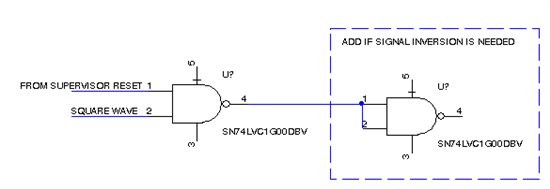
    One other thing I neglected to mention.  It really is not a good idea to modulate the PWRDN pin.  I would suggest something like a single NAND gate, or a dual NAND if you need a signal inversion, to isolate the signals from each other as shown in the following figure.  Anything that needs a static signal for reset is controlled by the supervisor and can be isolated from the device requiring a square wave.  There are other ways of separating these signals, but the idea is that you really don't want to add what is basically noise to the reset pin of the device.


    Best regards,

    Bob B

  • MH,

    I really don't see any issues when using the header connector.  You could potentially have issues using the DB9 connector as there are possible resonant circuits.

    Best regards,

    Bob B

  • Hi ,

    In my study on the error sources of my design,

    I have seen a  semi_error in Application cicuit Figure_42 of  ADS1232 datasheet , page 25

    SBAS350F–JUNE 2005–REVISED FEBRUARY 2008

    based on specs of Page 3: Common-Mode Input Range   Gain = 64, 128      min= AGND + 1.5V    max=AVDD – 1.5V 

    ( I think in selected analog input...)


  • Cont...

    Page 25, Figure 42. Weigh Scale Application

    the gain is 128 , AINP2 , AINN2 are connected to AGND ===> The Common Mode Range is Violated

    the only reason can be : "the selected Analog Input Channel"  should have the Common Mode Input  Range  spec...

    regards

  • Hi Bob

    I did Check these items:

    ( in my tests :no offset calibration is used , else it is mentioned)


    1. AINP2 ,AINN2 , now are connected to AVDD/2 :  effect : the problem exist again.

    2. Stabelized clean  /PWDN : effect : the problem exist again.

    3. manually changed the gain between 64,128 : effect : the a2d readings at the same gain and same signal changes vastly

    ( a2d value @ g128 changes ~10,000  ) and the problem exist again.

    4. manually pull down the /PWDN then pull up it :  effect : the problem exist again.

    5. shorted AINP1, AINN1 together to AVDD/2 :  effect : the problem exist again. ( a2d reading is near  -8000 +- 250 )  after offset calib it changes to 0+-50

    6. removed the XTAL and grounded one pin for internal oscilator. : effect : the problem exist again.

    7. and I touch randomly the pads of parts when the system is on, and because of my body electrostatics and other noises , a2d changes the unwanted offset to zero !!!!

         this test is done on 5 pcb's and many times....( I know the bad effect of touching the CMOS devices....but I am testing anything)

    8. the inputs AINP1,AINN1 shorted together and connected to a 20k_potentiometer (two ends of pot connected to AVDD,AGND) and the a2d readings for

        different Vcm(Common Mode) are here: ( I Know for g128 the Vcm must be in the rage of (AGND + 1.5V) to (AVDD – 1.5V) ) but for test:

    Vcm a2d

    5.000 -2040 +-10

    4.500 -2030 +-10

    4.000 -5800 +-25

    3.500 -5950 +-30

    3.000 -6770 +-30

    2.500 -7950 +-30

    2.000 -8975 +-30

    1.500 -8940 +-30

    1.350 -12750 +-30

    1.250 -7200 +-30

    1.000 +3950 +-20

    0.500 -51300 +-100

    0.000 +83500 +-1000


    for Vcm from 1.500 to 3.500 ( the acceptable Vcm range in gain of 128 )  the readings (of zero volt diff input) are unstable .....

    9. by shorting +SEN to AVDD , -SEN to AGND  on PCB and cutting the +-SEN wire of  loadcell :  effect : the problem exist again.

    10. I have already designed the same size a sample PCB and by using same Parts , but a2d is AD7780 from analog devices,

    and same connections(DB9F-RA , SIP-7 , SIP-8 ...)

    By changing the software code I can read AD7780 without any problem ( 24bit and 150,000 stable loadcell reading at 10hz )!!!

    all parts are the same and pcb is changed slightly for AD7780 smd.

    11. I will disassemble the DB9, and will remove some of them from pcbs for testing the effect.

    , and I did this and ,  effect : the problem exist again.


    and one point:

    I recieved other PCB that has ADS1232 on it ( but the printed writings ot top side of ads1232 is differ from my ads1232 parts.

    it has normal gray colored tampo printing 

    but some of my parts have etched nocolor printing on them,(L1:ADS132     L2: ti  53T    L3: EOFX)

    which TI production site is the source of my parts?


    the second point

    after some experiment , after a turn on of system , the a2d reading of (Zero input at Vcm_2.5v), became  3,388,100   +-50  !!!! and it remained and not chaged by turn off and on , 

    then I walked through my office and then touched the AGND , and the huge static electricity discharged to pcb,

    then ............... the unwanted offset disappeared ( it changed to near zero value )

    then a turn off and on again! the -8000 +-200 affset appeared again.


    and some question,

    ?1?  Is it possible to be some sort  of  Electric Charge trap ( such as burried gate in EPROM , EEPROM...in insulation layer ) in the ads1232 design / fabrication process?

    ?2? Why this device is too sensitive to EMI?( at least in my PCB's )


    ?3?  Is it possible to send my pcb_samples to TI for testing them???

    ?4?  Or ,am I recieved the original ads1232 parts?

    ?5?.  Is it possible to recieve the original parts / samples in Middle Asia? ( not from china )

    ?6?  What are the other users of this a2d  experiences?


    regards


  • MH,

    You are correct about the common mode input range being violated if indeed you were trying to measure the inputs.  The reference design you are referring to does not ever read the AIN2 inputs, and thus the mux is never connected to the PGA.  It is always a good idea to connect floating inputs to something.  Usually the easiest place to connect is ground.

    Best regards,

    Bob B

  • MH,

    There is a lot of information to digest from your latest post.  Let me try to make a couple of points clear.  The first is that all delta-sigma parts have issues with offset from the modulator that needs to be calibrated out.  You should always run the offset cal and this should be your baseline measurement.

    Also, it would appear that you have some grounding issues.  It is always a good idea to join the grounds for the analog and digital portion very close (even under) the device (ADS1232.)  Long ground traces are not a good idea.  Nor is it a good idea to use an inductance of any type to bridge the grounds together.  We have found that a single ground plane works very well as long as the analog and digital portions are not crossing over each other.

    The device is sensitive because it is designed to be sensitive.  A very high input impedance will respond to a very small charge.

    Did you ever place the caps at the supply pins for bypassing as well as a bulk capacitor across the reference?  Without these caps you will never get the performance you desire.

    Best regards,

    Bob B

  • Hi Bob,

    The PCB includes  0.1uf ML cap for DVDD,DGND (Cs5) Close to pins1,2

    and  0.1uf ML cap for AVDD,AGND (Cs6) Close to pins 17,18   plus a 100uF  electrolite cap ( CEA2 )


    and new questions:

    ?7? . What does happen , when the AVDD has delay  after DVDD becomes stable at 5.0 volts ( a delay of 1 sec ) or vice versa?

    ?8?.  What does the device do when we insert extra 27th and 28th and... SCLK immidiately after 26th SCLK ( without waiting for complition of internal operations ) ?

    ?9?.  what does happen if some tracks routed under the chip body on the PCB( such as my case ) ?

    ?10?.  what are the behaviors of the device , when it is damaged by:

    - Over heating in soldering process by iron tip ?

    - Static Electricity of Body , in manual assembly ?


    ?11?.  In which conditions do I consider the device is damaged ?

    Regards


  • MH,

    At this point I'm not going to answer all of your questions because I think the real answer will get lost.  You have a serious analog issue that starts at the input.  First of all the regulator you are using has noise issues of about 200 micro-volts or more.  This will affect the stability of your readings.  However, the bigger issue is your analog ground.

    Basically you have one big antenna ground loop.  Notice the green trace I have shown on the top layer.  Ground traces are bad.  You should have a ground plane.  I think you you may have thought you have a ground plane because you have large copper areas.  Many of these copper areas are either not connected, connected through narrow traces, are in areas not vital to the ADS1232 itself. 

    Notice the long ground trace to the regulator ground.  The regulator ground path should be as close to the power entry point as possible, and capable of handling large currents.  Remember you are regulating 8.5V to 5V.  Also, the analog bulk capacitor ground has the same issue.  All currents end up going right past the ADS1232 ground. 

    Another thing to consider is the ferrite on the analog ground will choke high frequency noise, and that noise is also passed around the current ground trace that will affect stability and noise of the ADC reading.

    If you look at the bottom view of your layout, that I have attached drawn on, you can see how you can make a huge improvement in the analog ground.

    This is a start, but you still have a lot of other issues, including the digital ground, and the ground antenna loop around the crystal.

    Best regards,

    Bob B


  • Dear Bob,

    I realised that several members had the same problem I currently have regarding unpredictable startup offset behavior of ADS1232. I saw no real explanation for the problem. What MH Solsal described in 2011 was a big offset jump. It has surely nothing to do with zero drift. I am in the same trouble now. The zero point after starting up ( input  unchanged) can change even several percents of full scale. After start it keeps its value, so it is a kind of initialization problem. The 'zero jump' can be generated with quick swich off/on of our indicator. If we wait for several seconds before switch on, there is no offset jump. It seems like some internal registers are not initialised at power up or something like that. We are a weighing company having own development and production. We have experience with several strain-gauge frontend chips and had no similar problems before. First I thought that maybe our indicator firmware has a bug and makes power up value unstable. Later I realised that the A/D converter itself  generates the offset jumps, if repowering happens too fast. I wonder if there was any new experience since 2011 about this problem. We have to solve it somehow. Several scale companies are using the same chip. If they would face the same problem, they could not use it. Our chips came from China. Do you know about any low quality copies?  Maybe it is just a matter of  source of the chips ( we have about 100 pcs for first batch of production but we cannot release the product until we cannot find solution.)

    thanks in advance for any helping input

    regards,

    Miklos

  • HI Miklos,

    What is probably happening is the ADS1232 is not properly issuing a POR.  The POR will not take place if there is residual voltage still on the device.  This is often due to charge still held by bulk and bypass caps.  The discharge path is usually quite slow as compared to startup.  Sometimes adding a bleeder resistor will help to discharge the caps sooner.  The downside is additional current that is consumed in normal operation.

    Best regards,

    Bob B