This thread has been locked.

If you have a related question, please click the "Ask a related question" button in the top right corner. The newly created question will be automatically linked to this question.

ADS1113: Can't read & control an ADS1113 from the scratch

Part Number: ADS1113
Other Parts Discussed in Thread: ADS1115

Hi,

I'm little confused about how to control an ADS1113. I don't know if is a hardware or software issue, so I will start with the circuit.

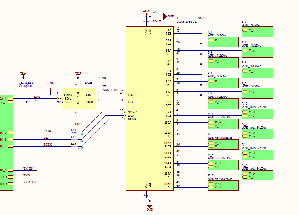
I tested that the multiplexer was working right, I'm using the S16A & S16B:

Test 1 -> I applied 3.3V to S16B and let S16A floating, the ADC returned me around 22300 counts (~ 2.8V), I tested with the multimeter the voltage on S16B, was 3.3V but when I tested on S16A the voltage was 1.23V How it can be possible?

Test 2 -> I applied 3.3V to S16A and let S16B floating, the ADC returned me around 22300 counts (~ -2.8V) negative, I tested with the multimeter the voltage on S16A, was 3.3V but when I tested on S16B the voltage was 1.23V too

Test 3 -> I applied 3.3V to S16B and GND to S16A , the ADC returned me around 32767 counts (~ 4.096V)

Test 4 -> I applied 3.3V to S16A and GND to S16B , the ADC returned me around 32767 counts (~ -4.096V) Negative

Test 5 -> I floating S16A  & S16B and measured voltage each pin AIN0 & AIN1 to GND, and each pin returned me 1.23V

Now, let's talk about the software, first I'm been using the ADS1115 python adafruit library, once I got that readings I'm tried with my own code, I get the same readings

import smbus
import time

bus = smbus.SMBus(1)

bus.write_word_data(0x48, 0x01, 54147)

time.sleep(1)

val_swapped = bus.read_word_data(0x48, 0x00)

val = (val_swapped & 0xFF) << 8 | (val_swapped >> 8)

I don't know what it's going wrong

  • ponchoM,


    First, I'll assume that you're making measurements with the S16A and S16B channel. When making measurements with the ADS1113, I would only make measurements when the inputs are defined. I would not float inputs while making the measurement. With a floating input, the ADC input could go anywhere. I'd also note that the input must also have a defined common-mode and the input voltages must be within the supply range from GND to VDD.

    All that being said, it still looks like you're getting some error in the readings. If as in test 5, you have AIN0 and AIN1 grounded and you still read 1.23V, then you have some error in the communications or setup. There are a couple things to look at. First, I would verify your configuration setting of the ADC. I would read back the Configuration Register for the device. You can do this following the I2C plots of Figure 15 and setting the address pointer to 01. This way you can verify that your write to the device has been correctly written to the configuration register.

    Second, I would also use an oscilloscope to verify the communications to the device. If you have some added capacitance on the SDA and SCL nodes, you might have some slow waveforms. The fact that you're getting some value is a good sign, but it would still be good to look at the waveforms. You can also use this to verify the plots from Figure 15.

    I would also check the returned values from the inputs. If you redo test 5, check the inputs so that both are ground, can you collect a set of data (maybe 50 points) and collect them into a spreadsheet or text file. I'd like to see the raw data and not the value converted to voltage. I want to verify that you are correctly making the ADC conversion.

    Read through my comments, and get back with a few results. I'm sure that we can find a solution.


    Joseph Wu

  • Hi Joseph,

    Thanks for the reply, I couldn't do a test with the oscilloscope yet, but tomorrow I will do that.

    First I was working with a Raspberry Pi and python but now I'm testing with an arduino.

    Test 1:

    Code:

    You can find attached the arduino code that i'm using  for testing

    Circuit:

    AIN0 = GND

    AIN1 = GND

    Code response:

    Config register Initial State: 1000001110000011
    Conversion register Initial State: 0

    Writing 33667 to Config register
    Done!

    Config Register after writing 33667 to config register: 1000001110000011
    Conversion Regiser after write conifg register: 0

    Test 2:

    Code:

    You can find attached the arduino code that i'm using  for testing

    Circuit:

    AIN0 = 3.3V

    AIN1 = GND

    Code response:

    Config register Initial State: 1000001110000011
    Conversion register Initial State: 0

    Writing 33667 to Config register
    Done!

    Config Register after writing 33667 to config register: 1000001110000011
    Conversion Regiser after write conifg register: 111111111111111

    So, the data still be the same as on the raspberry, What other thing can be? The code is ok? 

    By the way the figure 15 in the datasheets that the TI website return me is a graph of Noise vs Supply Voltage.

    Hope you can see what i'm doing wrong

    ads1113.zip

  • ponchoM,


    It's hard to guess what the problem is with just the code. It's so much easier to look at the waveforms to see the exact SPI transactions to debug it. For now, I would get the oscilloscope and look at what's coming out on SCLK, DIN, DOUT, and /CS. Post the plots back into this thread and we can see what's happening.


    Joseph Wu

  • panchoM,

    I haven't heard from you for a little while, and I thought I'd check on your progress. In my last few posts, I mentioned that I wanted to see the SPI communication between the device and the master. This would include either oscilloscope plots or the output of a logic analyzer.

    Hopefully, you were able to solve your problem. I'll close this post for now, but if you continue to have problems, read through my posts again and post back to this thread. We can return to working on this issue.


    Joseph Wu