This thread has been locked.

If you have a related question, please click the "Ask a related question" button in the top right corner. The newly created question will be automatically linked to this question.

ADS1278-SP: Stress on device with out digital I/O

Part Number: ADS1278-SP
Other Parts Discussed in Thread: ADS1278

Hi Team,

My customer is having a test case where +5VA of ADS1278 is present along with analog inputs but +3.3VD, +1.8VD and all Digital I/Os are not present for 1 hour. Can this condition stress the device. Can any degradation happen to device.

Regards, Shinu Mathew. 

  • Hello Shinu,

    As long as the customer does not exceed the ABS Max ratings, then there should not be any long term degradation to the device.  However, they are not meeting power up requirements, so it is suggested to bring AVDD to ground (as well as the analog inputs) and then follow the power-up sequence outlined in Figure 85 of the datasheet.

    Regards,
    Keith Nicholas
    Precision ADC Applications

  • Thanks Keith,

    Thanks for the inputs.

    Regards, Shinu.

  • Hi Keith,

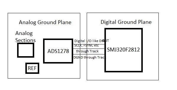
    Attached is the grounding scheme customer is planning for the new PCB. Can you please comment whether its ok to prevent loss of ADC accuracy and ground coupling. Please help with your inputs.

    Regards, Shinu Mathew.

  • Hi Shinu,

    For the ADS1278, it is extremely important that AGND and DGND are connected to the same analog ground plane directly next to the device.  Ideally, connect AGND and DGND to the thermal pad and then use multiple vias between the thermal pad and the analog ground plane.

    You can maintain separate analog and digital ground planes for the rest of the system, but they should be connected together beneath the ADS1278 with a wide connection, not through vias to a shorting resistor or a shorting trace.

    Please note that the best EMI performance will be with a single ground plane.  The above placement of analog components on the left side of the board and digital on the right side should perform well, keeping analog and digital currents separated for best noise performance.

    Take a look at this FAQ that describes the different options.

    https://e2e.ti.com/support/data-converters/f/73/p/755516/2790926

    Regards,
    Keith

  • Hi Keith,

    Thanks for the inputs.

    Shorting at 7.0380 mm thermal pad below the device, that means all the DGND and AGND of the ADC should be routed in the top layer (Layer-1) below the device and connected to the heat pad. Then the heat pad connections to be made through multiple vias to the below analog ground plane (Layer-2). How many vias to be provided typically ?.

    If customer is following the above scheme then statement "You can maintain separate analog and digital ground planes for the rest of the system, but they should be connected together beneath the ADS1278 with a wide connection, not through vias to a shorting resistor or a shorting trace" is not valid, correct? 

     Thanks for the support and suggestions.

    Regards, Shinu Mathew.

  • Hi Shinu,

    A convenient way to tie all ground pins together is through the thermal pad, but you can use individual via's as long as they all tie into the same ground plane.  For the commercial version, we recommend 9 vias in the thermal pad area tied to ground.  However, this is just a recommendation.

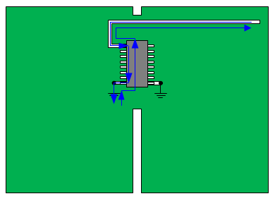
    What I meant by the above statement is that you can have an analog ground region, and a digital ground region, but they must be tied together beneath or very close to the device.  The below Picture is what I am trying to describe; it is a single plane with slots to separate the two regions.  This really is a single ground plane, but it is divide into analog and digital regions.

    Regards,
    Keith

  • Hi Keith,

    Thanks for the brief.

    Regards, Shinu Mathew. 

  • Hi Keith,

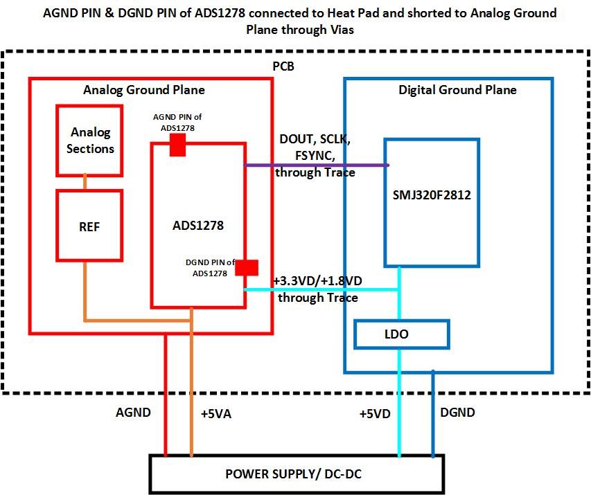
    Need one more clarification, in that case how the digital supplies of ADC (+3.3VD, +1.8VD and its decoupling capacitors) get the ground reference. Do we need to short the AGND and DGND at card end or power supply (which may be upto 10meters away from the PCB). Please refer attached  image for reference.

    Regards, Shinu Mathew.

  • Hi Shinu,

    The analog and digital grounds need shorted on the card end.  You can run separate ground returns for each supply voltage as shown above, but there should be a solid ground connection on the board itself.  Also, to minimize radiated EMI from the digital lines, the digital ground plane should extend beneath the IO lines and connect to the AGND plane near the ADC.  

    Below is the suggested ground layout, which is similar to my previous post.

    Regards,
    Keith