This thread has been locked.

If you have a related question, please click the "Ask a related question" button in the top right corner. The newly created question will be automatically linked to this question.

ADS5263EVM: Set registers through test points, not through USB

Part Number: ADS5263EVM
Other Parts Discussed in Thread: ADS5263

Hi,

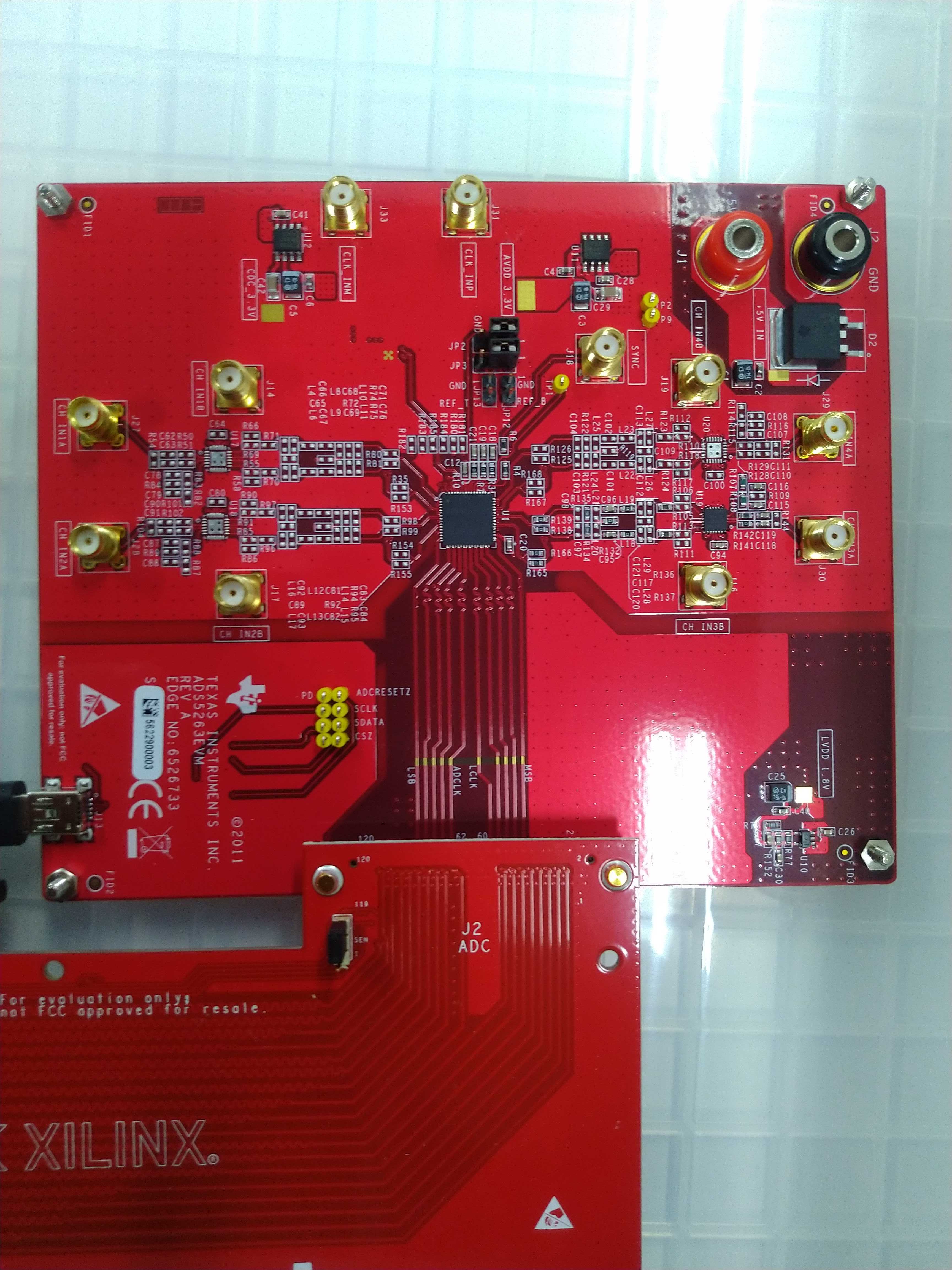
I'm using ADS5263EVM and now trying to configure the registers of this ADC through serial interface. Test points TP13-TP16 on EVM are connected to the ADC, but these are also connected to FT245RL.

May I use these test points to feed serial configuration signal from FPGA?

Of course, when I feed serial configuration signal from FPGA, I plug off the USB cable. But I'm worrying about whether feeding signals from the test points harms the FT245RL or not.

Thank you,

Yoshitaka

  • Hi,

    Thanks for using ADS5263EVM.

    Yes, please use these jumpers

    (such as

    TP17=SDOUT,

    TP14=CSz,

    TP12=SDATA,

    TP13=SCLK)

    by connect them to "USB SIDE" side or the other side (will be connected to J8 connector for FPGA usage) or

    to any your own test points,

    for you to connect them to control the serial interface.

    Please look at the ADS5263EVM Users' Guide.

    Hope that can show you the schematics of this EVM.

    Thank you!

    Best regards,

    Chen


  • Hi Chen,

    Thank you for the reply.

    The problem is that my board doesn't have such jumpers. I attach a picture of the board I have

    ADS5263EVM I bought

    The version of this board is REV A 2011. We only see the yellow test pins at the left bottom of the board.

    On the other hand, a picture in the User's guide of ADS5263 is a little different from mine. Here's a cropped image of the board in Figure 1:

    As a white circle shows, the picture of the board in the ADS5263 User's guide has such jumpers. And in Figure 9,

    We clearly see selection jumpers in the board. Enlarging the image, the revision of the board seems REV B.

    Furthermore, the schematics in the guide has no such jumpers. Here's the cropped schematics of the board:

    The named signals, sclk, sdata, csz, adcresetz, and pd are directly connected to the chip.

    The schematics shown in the user's guide are consistent with my board, but inconsistent with the board in Figure 1.

    My board have four jumpers, named JP12, JP13, JP2, and JP3. However, none of them are related to the serial interface. So I cannot apply your advice to my situation.

    Maybe we have several versions of ADS5263EVM in the market? I did not have version options when buying.

    Do you have any workaround to solve this?

    Thank you,

    Yoshitaka

  • Hi Yoshitaka-san,

    How are you?

    Thank you so much for your very detail information.

    Very sorry, the ADS5263 EVM is an older version (we are using REV. B now).

    Yes, I need to ask my manager and will let you know quickly.

    Thank you for using ADS5263 device.

    Best regards,

    Chen

  • Hi Chen,

    It's kind of you that you process this problem quickly. Thank you.

    Okay, I'm looking forward to receive any updates.

    Best regards,

    Yoshitaka

  • Hi Chen,

    How are you?

    How about the situation? Do you have any updates?

    Best regards,

    Yoshitaka

  • Hi Yoshitaka,

    How are you?

    Here is the answer from our manager:

    -------------

    The central repository server for the EVM files (CDDS) only has rev A.

    There was rev B built probably one time and probably the version that this customer has is from the new build (rev A).

    The schematics in the user guide refers to Rev. A.

    --------------

    so now we have only Rev. A.

    sorry for the inconvenience.

    Thank you!

    Best regards,

    Chen

  • Hi Chen,

    How are you? Thank you for sharing the updates.

    Then, my first question, "Set registers through test points, not through USB" is not possible with the board I have (Rev.A). Is this correct?

    Best regards,

    Yoshitaka

  • Hi Yoshitaka,

    How are you?

    sorry, it is not possible with the board rev A you have

    unless the followings needed to be modified:

    1) need to remove R188-R192

    2) by soldering wires, connect TP12-TP19 to J8 Connector.

    3) also connect SDOUT pin from DUT to J8 Connector

    for readout purpose.

    Thank you!

    Best regards,

    Chen

  • Hi Chen,

    Thank you for your help!

    I understood how to modify the board for this purpose.

    However, the pins of J8 connectors are too small to solder by hand (in addition, unused pins are connected to GND), so I will connect them directly to the FPGA board.

    Best regards,

    Yoshitaka