This thread has been locked.

If you have a related question, please click the "Ask a related question" button in the top right corner. The newly created question will be automatically linked to this question.

ADS1256: ADS1256

Part Number: ADS1256
Other Parts Discussed in Thread: OPA350

Dear TI Team,

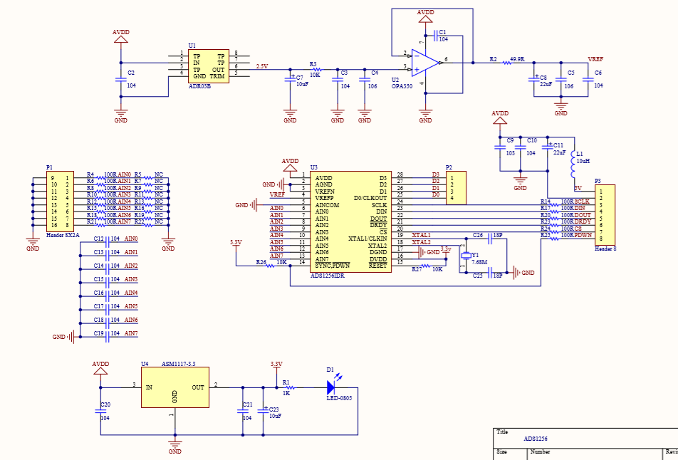
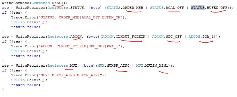
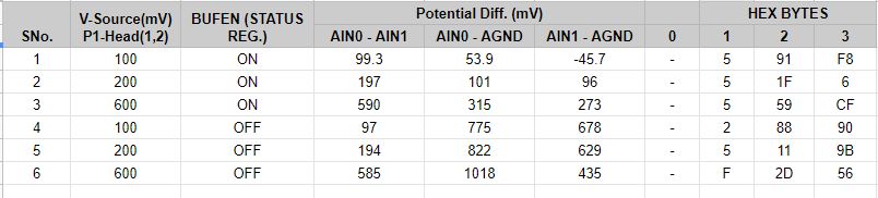
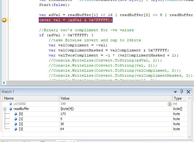
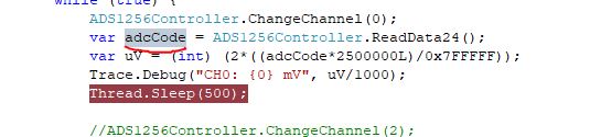
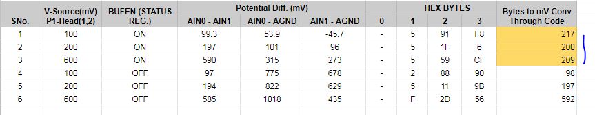
We are using ADS1256 for measuring Differential Analog input, But we are facing one problem. When BUFFEN register is ON we are not getting proper ADC reading above 200 mV from the ADC , But after disabling BUFFEN register we get acceptable ADC reading. We are proving the analog input from a voltage calibrating device. Kindly Let us know what is causing this problem.

I am adding the Configuration details bellow:

1. VRef. : 2.5V

2.Gain : 1

3. ADC I/P : Differential Analog

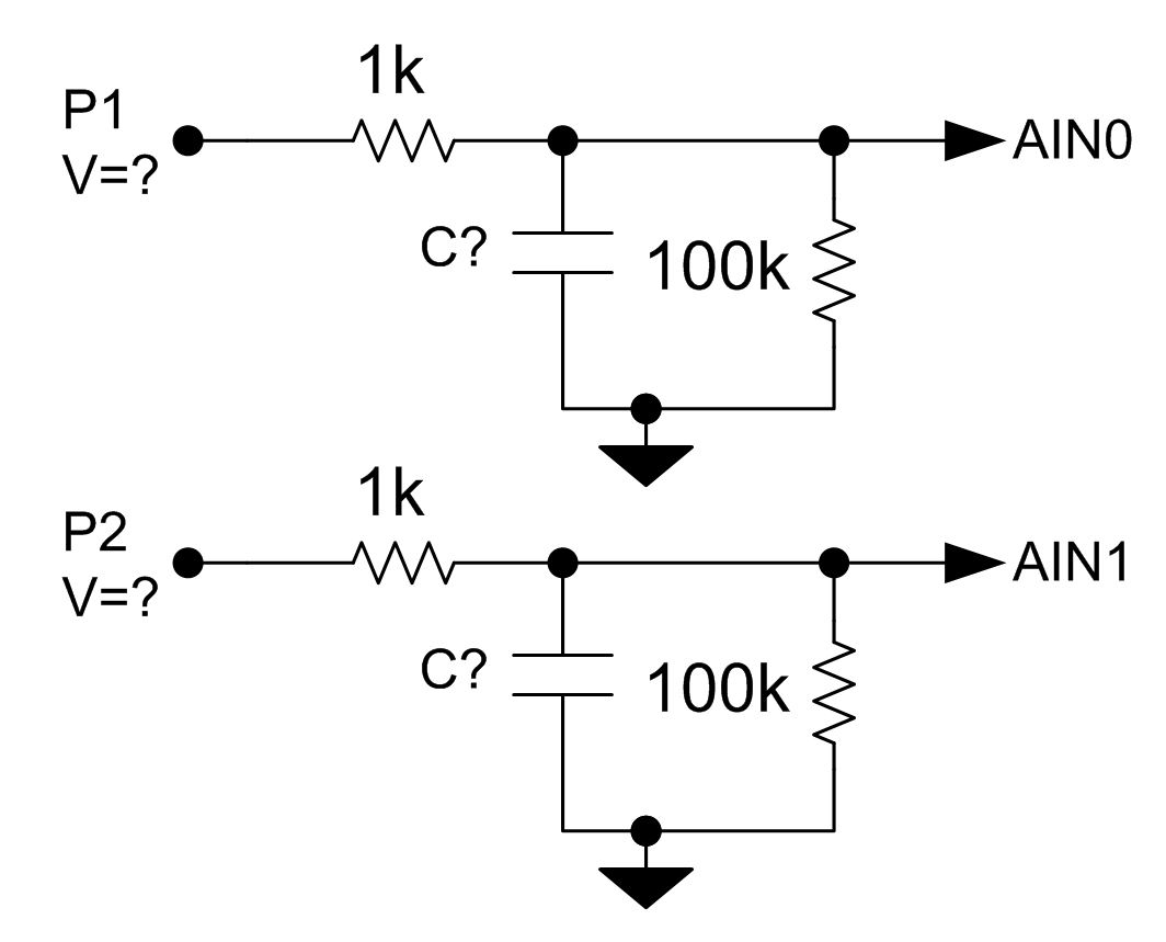
4. Input channels are biased with 100 K resistor.

  • Hi,

    Can you provide a few more details to help diagnose this issue:

    • Can you share a schematic?
    • What is the input voltage to the ADC from the calibrator? You said "200 mv", but is that referenced to GND or some other bias voltage?
    • What do you mean by "not getting proper reading"? Are you getting no data at all, or are the codes clipping, etc.?

    Let me know.

    -Bryan

  • Dear Sir,

    I am adding the schematics of the ADC board.

    We want to use this ADC for measuring Differential voltage, for that purpose we have connected analog voltage source, between AIN0 & AIN1 (*Header P1 / Port : 1,2 ) , Also we have populated R5 & R7 with 100 k (*Which are Biased to GND). The Vref is of 2.5V. All the series input resistances is of 1k instead of 100 ohm (*R4,R6,R8,R10...)

    We are getting the wrong ADC count bytes (*clipping!)  with respect to applied voltage above 200mv from calibrator. below 200 mv byte counts are fine with BUFFEN on. We have observed that when we are turning off the BEFFEN we get proper ADC Count bytes.

    Sir, Kindly let me know if you need more information.  

  • Hi,

    Can you please clarify how you are applying a voltage to pins 1 and 2 and P1, and what those voltage levels are? Is 200 mV a differential voltage e.g. AIN0 - AIN1?, or is that single-ended referenced to AGND?

    Also, what is the ADC data rate, and what is the cap value on the input e.g. C12, C13, etc.

    This is how I am interpreting the input structure to the ADC and where you are tapping the input to the ADC. Let me know if this is incorrect, and if you can clarify the voltages and cap values as shown.

    -Bryan

  • Dear Sir,

    200 mV applied as a differential voltage between AIN0 - AIN1, through RC network similar to that you have drawn above.

    ADC data rate  :  30,000SPS (default)

    Cap value        :  0.1uf

  • Hi,

    What is the absolute voltage at P1 and P2? The voltage between these points is 200 mV, but does P1 = 2.5 V and P2 = 2.3 V?

    -Bryan

  • Dear Sir,

    What we are planning is to use the ADC to measure +2.5V to -2.5V analog signal, so initially when we are testing, we have applied 200mV signal, means P1 is at 200mV and P2 is at 0V (*which are connected to ADC channel 0 & 1 respectively). The thing is if we don't change any thing in the hardware & analog input side just by disabling the BUFFEN register then it will result in a positive way, after that we get proper ADC counts. But we need BUFFEN option.

    Regards,

    Harinder Singh

  • Hi Harinder,

    I don't see anything obviously wrong with your schematic given the information you've provided thus far. The resistor in the OPA350 output path will cause a small gain error due to the voltage drop across it, but that would not be a sufficient reason for this issue. Can you post your register settings so I can review them?

    Also, can you confirm there is no ground potential between the calibrator ground and the PCB ground (AGND)? If there is a few volts difference this could certainly cause the error you are describing. It would be helpful to check the voltage on P1 and P2 relative to AGND to make sure they are in fact 200 mV and 0 V, respectively.

    Finally, if you can send the raw ADC codes (in hex) you are getting from the ADC under both circumstances, that would help as well. Thanks!

    -Bryan

  • Dear Sir, 

    I have made the following observation.

    Test Case / Note:

    1. Input analog voltage source is provided from calibrating device, which is powered by own battery so their is no common GND. between ADC board & Calibrator. AGND(* pin 2 ) of adc IC is connected to GND of the ADC board.

    2. Input Source is applied at P1-Header between pin 1 & 2. Due to series resistance their is some drop but that is fine.

    Register Settings during initialization of ADC.

    Observations :Hex byte is as per readBuffer array.


    Hex Byte conversion in the code. (*readBuffer Array)

    var adVal = readBuffer[1] << 16 | readBuffer[2] << 8 | readBuffer[3];

    Hex Bytes to uV / mV Conversion : adcCode will contain the return of HEX byte conversion .

    Sir, if BUFFEN of status register is OFF then we get everything fine. Kindly let us know what can cause such problem when it is Enabled.

    Regards,

    Harinder Singh

    M2MLogger

  • Hi Harinder,

    I am confused by the result shown in the table in your last reply. You had told me that for the 200mV measurement, P1/AIN0 was at 200 mV and P2/AIN1 was at 0 V (GND). So when you measure between AIN1 and AGND for example, the result should always be 0V, since both points are tied to the same potential. But you are showing >600mV in some cases - how is that possible?

    The table also shows that the differential measurement result is the same (and close to the expected value) whether the buffer is on or off. Are these results measured with the ADC or are you measuring them with a multimeter or other external tool? What do the hex bytes in the table correspond to? Three bytes would represent one 24-bit value, so it is not clear which voltage value in the table goes with which hex value.

    Please help explain the results you have posted.

    -Bryan

  • Dear Sir,

    This is the Basic Block Diagram of our Setup.

    Hex to byte Conversion Table : Sir, As you can see byte conversion is not correct for BUFEN enable. 

    We are using mutimeter to measure the voltages.

    Regards,

    Harinder Singh

  • Hi Harinder,

    For the first three cases in your table, one of the inputs must be below ground in order to get the differential voltages shown between AIN0 and AIN1. You show this in the first row where AIN1 = -45.7mV relative to GND. I am guessing AIN1 is <0V in all three cases, though it is not shown in the table. Otherwise, for row 2 for example, you should be getting AIN0-AIN1 = 101mV - 96mV = 5mV.

    Please note that the ADS1256 cannot measure voltages below AGND when the buffer is enabled, though it can measure down to AVDD-0.1V when the buffer is disabled. Are you able to level shift AIN1 up a few hundred mV to make sure you are within the operating range of the ADC?

    -Bryan