This thread has been locked.

If you have a related question, please click the "Ask a related question" button in the top right corner. The newly created question will be automatically linked to this question.

ADS54J60: Deterministic Disparity Errors While Receiving ILA Sequence with VC707 / Xilinx JESD Core

Part Number: ADS54J60
Other Parts Discussed in Thread: LMK04821, , ADS54J66, ADS54J66EVM

Dear all,

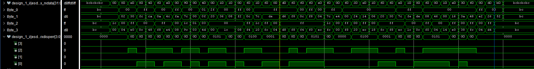
we are having trouble establishing a link between the ADS54J60 converter and a XIlinx VC707 board. We have checked the physical links (SYNC, SYSREF) and the eye diagram on the receiver side and see no issues. CGS is achieved and the converter begings the transmission of ILAS after SYNC is de-asserted.

Starting from octet 3 of the ILAS, the FPGA reports a disparity error on every other octet and consequently re-asserts SYNC shortly afterwards, causing the converter to transmit /K/ again. The link then gets stuck in this state.

The current test procedure is: Start device clocks and continuous SYSREF (LMK04821), put receiver into reset state, reset and configure converter, release receiver from reset state. Putting both devices into continuous /K/ test mode results in no errors.

The problem persists in subclass 0 mode, for a single-lane receiver and for pulsed SYSREF operation. Scrambling is disabled. Any further debugging advice is highly appreciated, especially regarding these two points:

1. What are the expected octets during ILAS? Some converters fill the in-between data with a counter value, but we are receiving seemingly random data (apart from the control characters and the JESD config data in the second multiframe).

2. There is no information in the datasheet regarding the supported values for K. We receive ILAS e.g. for K-1 = 15 but not for 31.

Best regards,
David

  • David,

    See if this helps (see attached). This is an example with our TI ADS54J60EVM interfacing with a VC707. The configuration file used by the ADC and LMK device is attached. The sample rate used was 983.04MHz. I also attached a signal tap capture of the 8 lanes during ILAS.

    K can be between 1 and 32 per the standard.

    Make sure that 17<K*F<1024 per the standard is meet as well.

    I would suggest you set the FPGA to ignore ILA errors as this is what most people do. I have seen issues with an IP (either RX or TX) not exactly following the standard or interpreting it differently, thus causing a ILA parameter mismatch, thus causing the checksum to have an error. 

    Regards,

    Jim

    LMK_983p04_VC707.cfg

     0728.LMF_8224_Fs_983p04M.pptx

  • Hi Jim,

    thank you very much for your support. I just realized I mixed up the part numbers in the question - we are seeing the problem with the ADS54J66; the ...J60 works fine in a different project.

    Note that the errors reported by the FPGA that lead to the re-sync are not about the actual content of ILAS (such as checksum) but related to the running disparity of the 8b10b decoder. If we manually force these error indicators to zero within the FPGA, ILAS completes and we are able to receive the correct data samples without (apparent) errors. However, I am not sure if we should do it this way in the final design - do you think this is some bug in the Xilinx JESD204 PHY / receiver core? Unfortunately, we cannot directly probe the raw 10b data before the encoder, so we cannot tell if the running disparity is actually wrong or just wrongly reported.

    Best regards
    David

  • David,

    I would try the following tests to see if you fix this error:

    1. Run at a slower data rate.

    2. Try running with subclass 1.

    3. Try increasing the size of the elastic buffer. Just make sure this does not get set to large as the release point my cross mutli-frame boundaries. RBD can be no larger than the K value.

    4. Trying increasing the K value.

    5. Which LMFS mode are you using and what ADC sample rate? Send us your ADC configuration file and I will compare it to what we use for this mode.

    6.  Is this error on all lanes? Have you tried running 2 lane mode?

    Regards,

    Jim

  • Hi Jim,

    thank you for your suggestions.

    1. We cannot easily decrease the line rate because of the connected logic, but I think we can rule out signal integrity issues on the basis of the eyescan and the deterministic nature of the error.

    2. The problem exists in both subclass 0 and 1 mode.

    3. Incresing RBD does not change the behavior. The error also occurs in a single-lane link, so I think we can rule out issues with the elastic buffer. For multi-lane links, the FPGA also reports that all arrival times are well within the safe LMFC window.

    4. The error occurs even for K = 32.

    5. We are using LMFS 4421 with a sample clock of 500 MHz and a linerate of 10 GB/s. The configuration is done in our firmware so I don't have a configuration file, but we double-checked all register values with the EVM GUI and the start-up procedure in the datasheet.

    6. The error is present on all lanes, we have tried single-, dual- and quad-lane links and also configured the receiver to disable individual or combinations of lanes, but the errors do not change.

    There seems to be a similiar (unresolved) issue with the ADS54J66 generating disparity errors:
    forums.xilinx.com/.../880824

    We have performed a full RTL simulation of the problem using the ILA octets received by the ADC as a stimulus. If the data is encoded correctly, there are no errors reported by the FPGA:


    However, this is what we see during ILAS from the ADS54J66 (the ordering of the bytes is reversed in the screenshot):

    The disparity errors only occur in every other octet, every time, starting with the third octet of ILAS.

    Are you able to connect VC707 to the ADS54J66 in LMFS 4421 mode without disparity errors in the link?

    Best regards,
    David

  • David,

    I just ran our ADS54J66EVM with a VC707 using our TI TSW14J10EVM interposer board. The interposer board passes all of the JESD signals between the boards. The main purpose of this board is to load the FPGA and capture data from the FPGA which then gets processed by the TI HSDC Pro software. All settings used are shown in the attached files.

    Regards,

    Jim

    ADS54J66_4421_bypass_mode_VC707.pptx3250.ADS54J66_bypass_4421.cfg