This thread has been locked.

If you have a related question, please click the "Ask a related question" button in the top right corner. The newly created question will be automatically linked to this question.

ADS1262: No DRDY pulse on power up and no SPI response

Part Number: ADS1262

Hi,

I have a problem with getting ADS1262 to work. The schematic of the ADC part of my device looks as follows:

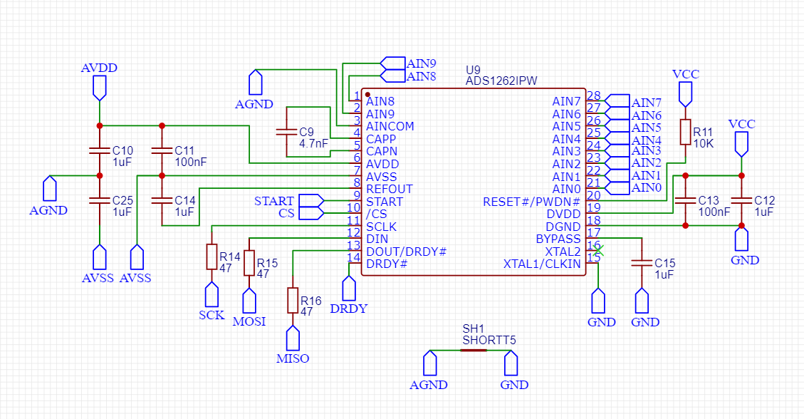
The chip is powered up, START pin is held high by the MCR, bo I observe no pulse on #14 (DRDY). According to the datasheet, it should pulse @20Hz after startup with #20 (RESET/PWDN) and #9 (START) pulled up.

I observe the following voltages (all measures with the respect to DGND):

DVDD on C13: 4.54V with peak-to-peak ripple of ~170mV

BYPASS on C15: 1.91V (22mV ripple p-p)

AVSS on C14: -2.03V (180mV ripple)

AVDD on C11: +2.48V (80mV ripple)

REFOUT on C14: -1.97V (180mV ripple)

This chip also does not respond to SPI and the analog voltage supply lines are very noisy, but I think the lack of DRDY pulse is the core problem that should be solved beforehand.  

Any ideas what's happening here?

  • Hi pa,

    Welcome to the TI E2E Forums!

    How are the AVDD and AVSS supplies being generated, and are they referenced to the same ground plane as DGND? If you have a more complete schematic that you can share it would be helpful (you can email it to pa_deltasigma_apps@ti.com if you prefer not to attach it to this thread).

    From your info, it looks like the "AVDD - AVSS" supply voltage is a little low (4.5V; minimum recommended analog supply voltage is is 4.75V). Also, REFOUT should have a voltage potential of AVSS + 2.5V, which might indicate that there is a bad connection somewhere.

  • Hi Chris,

    Thank you for the brief repply. I've sent you a complete schematic fo the device via email.

    Power supply reails are generated by TI LM27762DSSR dual power supply + LDO chip. I designed it to deliver +/-2.5V of supply for AVDD and AVSS, but indeed I see some soldering issues all over the board. Maybe I'll inspect this more thoroughly and get back with the findings ASAP.

  • Hi pa,

    Thanks for the schematic!

    Nothing stood out to be as a major problem. One minor issue I spotted was that the LM27762DSSR, which is generating the +/-2.5V analog power supplies is biased with respect to the digital ground, and as such all of this power supply's return currents will have to flow through the jumper back to digital ground. Hopefully this return path is short and low impedance, but it would be better to bias LM27762DSSR with respect to the analog ground.

    ...Even better yet, would be to have a single ground plane, as I wrote up in the following E2E FAQ:  [FAQ] PCB Layout Guidelines and Grounding Recommendations for High-Resolution ADCs. However, you might say I'm a little bit "biased" on this topic. ;)

  • Hi Chris,

    Thank you for the review of my schematic. Indeed, there's nothing wrong with it. I think I've found the issue, but not the solution so far. On page 6 of the datasheet there's a remark that input pins are diode-clamped to analog supply rails. The thing is that my detector arrays are sometimes overdriving the inputs.

    I have an array of photodiodes with transimpedance amplifiers powered with an external 0-5V power supply. Under normal circumstances diodes work in a fairly dark environment and the output of their op-amps never exceed +1V. But when exposed to ambient light conditions (which is the case during an assembly process etc), the output of transimpedance amplifier is saturated (+5V). This causes ADS1262 to clamp, power source goes crazy and bad things happen.

    Below is an outline of the detector schematic.

    Do you have an idea of how to handle this special conditions while trying to maintain as much of the dynamic range of the ADC as possible? I think the problem is with a proper signal conditioning stage. The signal of the detector is unipolar positive voltage that oscillates between 0 and 200 mV and occasionally goes beyond that to say +1V with some extreme conditions when the output saturates to +5V. Now the PGA of ADS1262 handles the most of the signal conditions (thus using only half of the positive voltage range), but during the overvoltage states the circuit becomes unstable.

  • Pa,

    I saw your post and just thought I would attach a document on photodiode amplifier noise.  I'm not saying you have an issue, but I know that it can be challenging to keep these amplifiers stable.  I hope the attachments are helpful.

    3833.noise11-Photodiode-Noise 1.pdf

    6242.noise12-Photodiode-Noise 2.pdf

  • Pa,

    In your design you are using bipolar +/-2.5V AVDD/AVSS for the ADS1262 the op amp can output as much as 5V. This will potentially exceed the absolute maximum ratings for the input to the ADC. You need to make sure that they limit any potential current to 10mA or less when in the over voltage condition. Perhaps a better option would be to use a bipolar supply on the amplifier so that an over voltage condition is not possible.

    There is a lot of good info on overvoltage in op amp and data converter video series (see links below).

    https://training.ti.com/eos-and-esd-adc?context=1139747-1140267-1128375-1139109-1137697

    https://training.ti.com/ti-precision-labs-op-amps-electrical-overstress-eos-1?context=1139747-1139745-14685-1138807-13956