This thread has been locked.

If you have a related question, please click the "Ask a related question" button in the top right corner. The newly created question will be automatically linked to this question.

ADS131A04: SPI slave STM32 readout missing a bit after changing ADC master SCLK frequency from 4MHz to 8MHz

Part Number: ADS131A04

Dear support,

Having successfully implemented a daisy chain of 2 ADS131A04 as depicted in Figure 99, we are running into trouble when using a single ADC in synchronous master interface mode.

Everything works fine in synchronous master mode until we send the command to run at a faster SPI clock. The ADC replies properly our sent commands, even once the high frequency SCLK is set but the slave buffer is shifted by one bit since the clock frequency change. The used microcontroller is a STM32F4. Since the MCU is configured as slave, there is no option to shift the Rx buffer other than per 8 or 16 bits.

The ADC is configured as master mode (M0=GND) and the DONE output is looped to the CSn input.

we used fixed word of 24-bit (M1=GND) and Hamming CRC disable (M2=GND)

The MCU settings are CPOL=0 and CPHA=1 (sampling on falling edge).

All this happens in configure device steps from flow chart Figure 109. Device not yet WAKEUP)

Is it expected to have the SCLK changing frequency in the middle of the next SPI frame?

Have you ever encountered such issue, any tips to solve this? Is there a specific precaution before changing SPI clock, such as ADC state or preliminary settings?

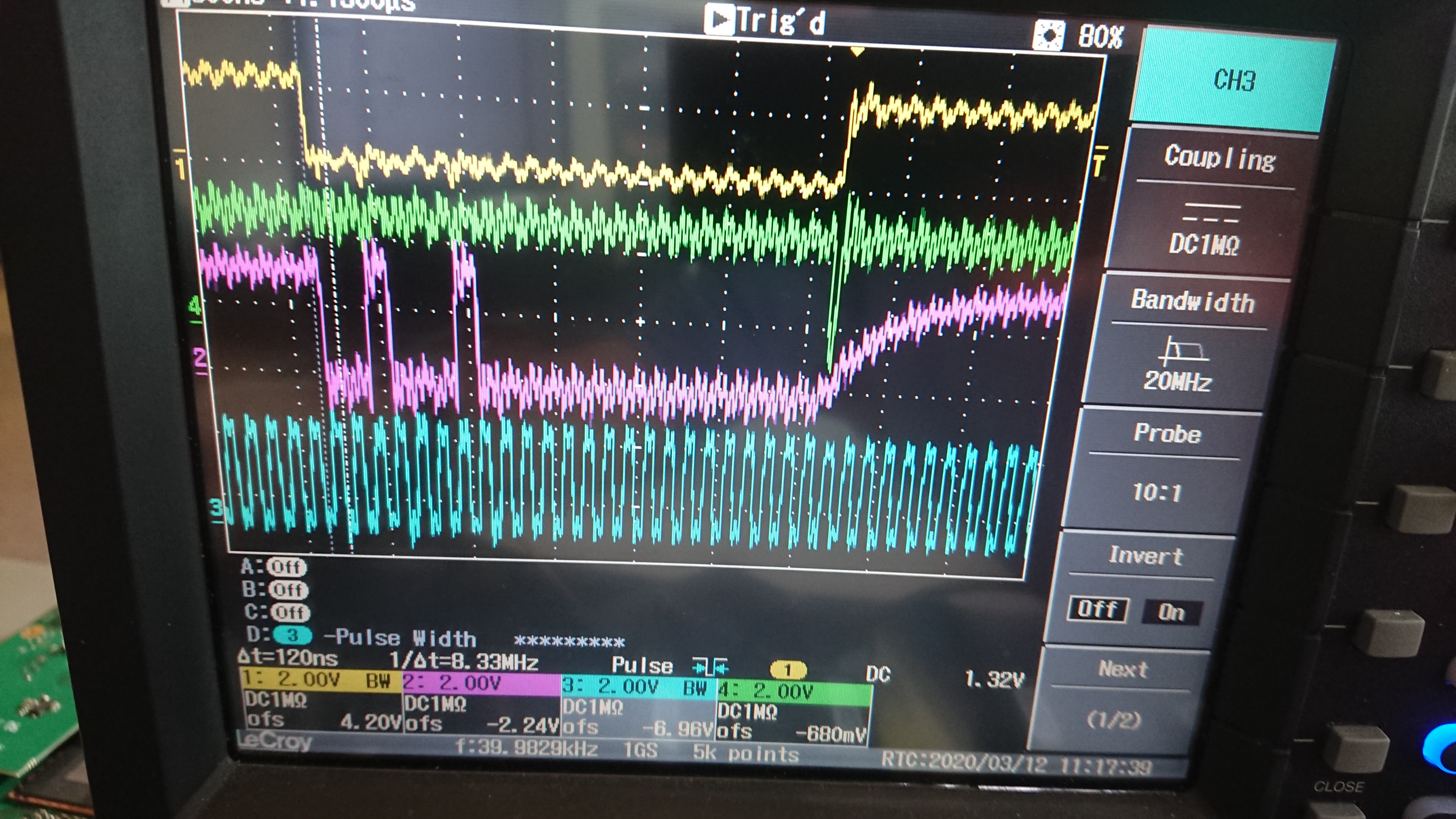
You can find attached the screenshots of the SPI bus signals.

ch1= DRDYn from ADC(MCU CSn)

ch4 = Done from ADC

ch2 = Dout from ADC (0x220000)

ch3 = SCLK from ADC (8MHz)

ch1= DRDYn from ADC (MCU CSn)

ch2 = Dout (0x2d0200)

ch3 = SCLK from ADC (4MHz to 8MHz)

Thank you ahead for your help!

Yannick

  • Yannick,


    To let you know, I've never seen this issue before. In master mode, the SCLK is derived from the ICLK signal that is divided down from the CLK_DIV setting. If this issue only occurs on the frame after the CLK_DIV write, can you insert a NULL to get past this error?

    Also, is the microcontroller having a problem with the read for more than just this frame? Even if the problem is the single wide SCLK, it looks like the data is correct. With the yellow trace as /CS, there should be enough time for the microcontroller to receive the SCLK. I'd note the response of 2D0200h looks like the fICLK has been set to 8MHz with fCLKIN/2 from 2MHz with fCLKCIN/8 which is the default (I can't see the time/div for the scope, but it looks like a change by a factor of 4).

    Can you provide your startup sequence? I just want to go through it and see what was written to the device and in what order.


    Joseph Wu

  • Joseph,

    You are right, this is going from default fCLKin/8 to fCLKin/2. The REFCLK is 16MHz (from MCU). (sorry for the mistake in the thread title from 4NHz to 8MHz).

    The missing bit only occurs for this frame, all other following frames receive 24 bits data.
    I am not sure if the last bit is not clocked by the MCU or the first clock of the next frame is not clocked by the MCU. The first is assumed (see attached screenshot of the first following frame after SCLK clock changed).

    first frame after changing clock SCLK

    ch1= DRDYn from ADC(MCU CSn)

    ch4 = disconnected

    ch2 = Dout from ADC (0x2E2900) , response to CLK2 register write

    ch3 = SCLK from ADC (8MHz)


    The startup sequence applied is the following, but we think that it would even occur without accessing A_SYS_CFG and D_SYS_CFG. 

    static uint8_t adc_config[] = {

    0x00, 0x00, 0x00,  // NULL
    0x00, 0x00, 0x00,  // NULL
    0x06, 0x55, 0x00,  // UNLOCK
    0x4B, 0x6F, 0x00,  // A_SYS_CFG
    0x4C, 0x3C, 0x00,  // D_SYS_CFG
    0x4D, 0x02, 0x00,  // CLK1
    0x4E, 0x29, 0x00,  // CLK2
    0x00, 0x00, 0x00,  // NULL

    };

    I have the idea the the MCU does not like the change of clock during the serial transfer. 

    With kind regards,

    Yannick

  • Yannick, 

    For your configuration commands, what is the response from the device in each of the following frames? The ADS131A04 is very specific about what the response is for each command. For your startup sequence, you have:

    NULL 

    NULL

    UNLOCK

    WREG A_SYS_CFG

    WREG D_SYS_CFG

    WREG CLK1

    WREG CLK2

    NULL

    For each of the commands, the following word should have given the proper response and I wanted to verify the response received during each write transaction. Can you list the response for each of the commands?

    Additionally, I wanted to check to see if you changed the order of the write, would you skip over this error? Instead of this sequence, could you use:

    NULL

    NULL

    WREG CLK1

    NULL 

    WREG CLK2

    NULL

    WREG A_SYS_CFG

    WREG D_SYS_CFG

    NULL

    With this sequence, you would send a NULL after each change of the clock, allowing all the other writes to be at a settled clock value.

    Joseph Wu

  • Hello Joseph,

    Thank you for the heads up, here below the readout. But  eventually I suspect the problem lies in the MCU SPI peripheral.

    The problem must come from the STM32F42x . There is an issue which can be related to the fact the the SCLK varies during teh frame which is not supported by the SPI slave...

    sent NULL (0x000000)
    received  (0xff0400)

    sent NULL (0x000000)
    received  (0xff0400)

    sent UNLOCK (0x065500)
    received  (0xff0400)

    sent NULL (0x000000)
    received  (0x065500) UNLOCK
    sent WREG(0x4D0200)
    received  (0x002200) STANDBY

    sent NULL (0x000000)
    receive (0x2d0200) WREG
     
    sent NULL (0x000000)
    received  (0x0044) STANDBY shifted by one bit
    with kind regards,
    Yannick  
  • Yannick,

    Thanks for the comment. If the problem is in the STM32F42x, then I won't be able to help on that one..

    Looking at the sequence, It looks a bit off after the NULL where the UNLOCK response is received. However, I get the idea that the response to the STANDBY is shifted forward by a bit getting 0x0044. 

    I wasn't able to pull up the errata sheet from ST. I'm not sure if you can change the timing of the commands or by space them out further. I'll close this thread for now, but if you have further questions, you should be able to post back.

    Joseph Wu

  • Thank you for your time Joseph!

    For anyone interested, this is what happens and what to do. But first, I recall some tips for the community, this won't hurt ;)

    1) when things works at low frequency but at high frequency, timing is most likely in cause, either due to signal integrity (overshoots, delays, level), or the timings such as defined by manufacturers.

    2) putting a scope on the signals shows the real world. well you could interfere with your probe and not see everything with a poor bandwidth scope or even creating ground loops but in general you see pretty much what you get

    3) go back to the design and check that you are respecting all timings, put side by side timing diagrams of involved chips (master and slave in this case) and draw yourself diagram with all min/max constraints.

    4) dig into hidden specs, be aware that microcontroller peripherals work on peripheral clocks for instance.

    Now regarding this specific issue, the facts:

    - we were using STM32F4xx SPI as slave with CPOL=0  and CPHA=1 as suggested by the ADS131A0x datasheet.

    - SPI SCLK is 8MHz (provided by the ADS131A0x as SPI master, fICLK = fCLKIN / 2 (CLK_DIV=001)

    - The STM32F4xx SPI used is SPI2, connected to APB1 clock system, running at 40MHz. (Be aware that SPIx are not all internally connected to the same peripheral clock... check figure 4 of STM32F427 datasheet

    - the microcontroller requires a NSS setup time of 4 times TPCLK See Table 62 of STM32F427 datasheet. This translates in minimum 100ns for us, which is not respected when settings the ADS131A0x at 8MHz SCLK. Note that using another SPI peripheral like SPI4 won't help either since a minimum of 50ns is still not enough since at 8MHz the provided set up time is 125ns/2 - at least 20ns ( tp(SDR) characteristics of the ADC, in Master mode, see chapter 7.9 of ADS131A0x datasheet)

    - all of this makes that we starts reading out one bit too late, and we readout out data multiplied by 2 = shifted left by 1 bit.

    A solution:

    What we did is changing live (in the middle of the ADC configuration) the microcontroller SPI slave from CPHA = 1 and CPOL = 0 to  CPHA = 0 and CPOL = 1. 

    This gives us half a SCK period extra time for the NSS setup time and a proper SPI acquisition. What is still confusing is that this mode does not work at low frequency but anyone eager to dig into that is welcome.

    Best regards!

  • Yannick,

    Thanks for your detailed reply and answer. I'll close this thread, but if you have further questions, you should be able to post again. 

    Out of curiosity, can you say what your application is?

    Joseph Wu