This thread has been locked.

If you have a related question, please click the "Ask a related question" button in the top right corner. The newly created question will be automatically linked to this question.

DAC80508: Read the Device ID

Part Number: DAC80508
Other Parts Discussed in Thread: TMS570LC4357,

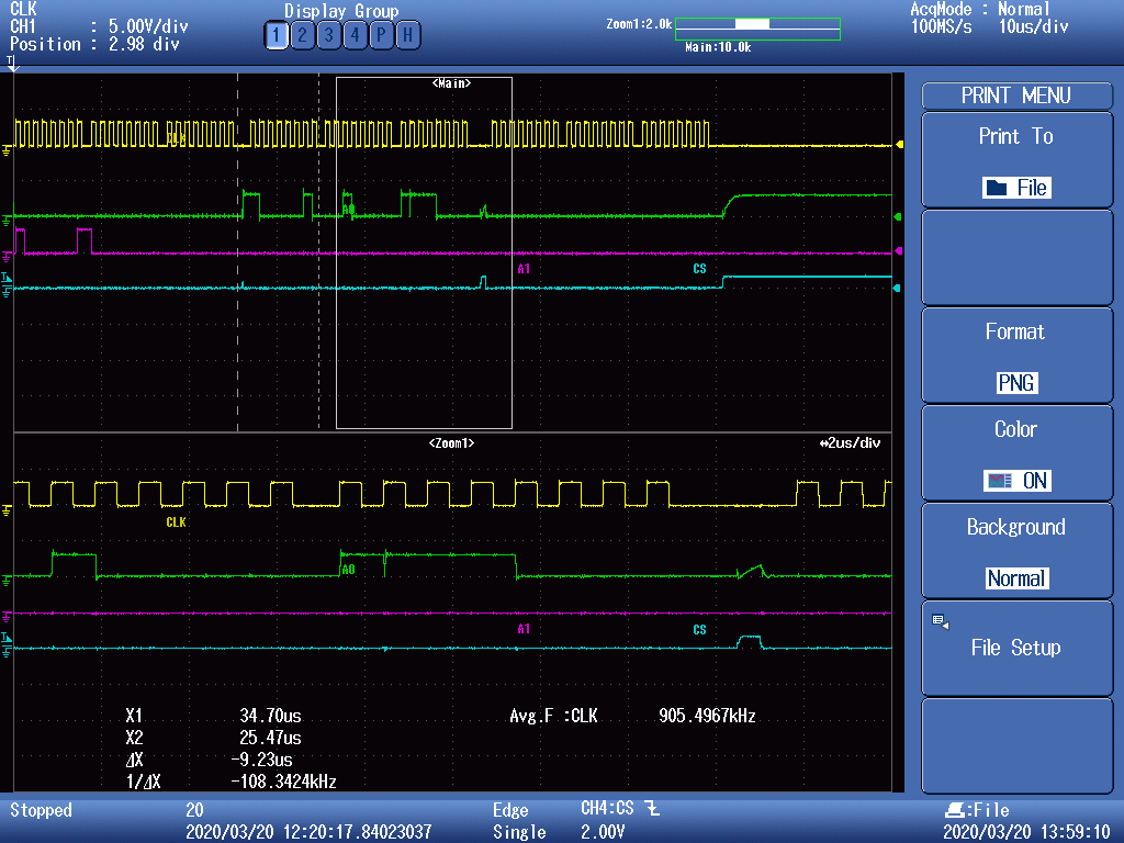
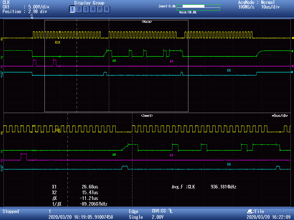
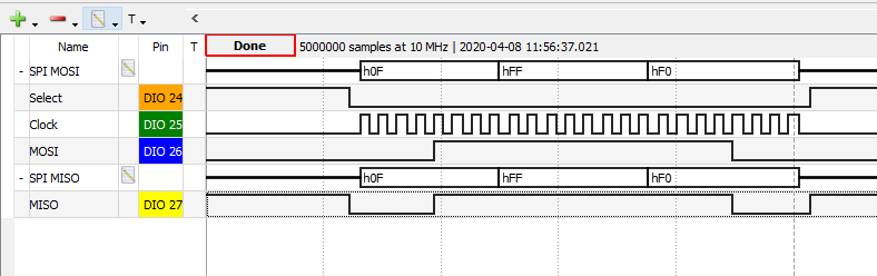
Hi, I am integrating the DAC80508 with TMS570LC4357 controller. I am using Evaluation modules for both the chips. Connections are made according the description in the data sheet. The SPI configured with 1 MHz clock (wanted to test with low clock speed initially). I have transmitted 24 bits (0x81 00 00) and try to read the SPI for two cycles. Attaching the screen capture of the SPI lines below.

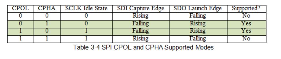
I have tried by changing the clock phase. There is no data output on SDI for the Tx on SDO with different clock phase.

As I understood from the datasheet, for the first read, it shall repeat the data I sent with transmit (echo) and 2nd read shall return actual data. The result does not look like.

Can you please tell me what I am doing some mistake?

The function calls are like below.

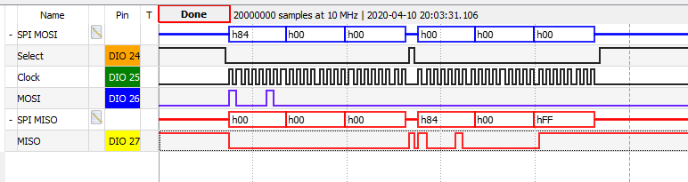
spiTransmitData(spiREG5, &dataconfig1_t, 3, tx_send_addr);//Device ID ADDRESS (0x810000)

//Delay

spiReceiveData(spiREG5, &dataconfig1_t, 3, tx_recv_data1); //1st Receive DATA (0x810817)

//Delay

spiReceiveData(spiREG5, &dataconfig1_t, 3, tx_recv_data2); //1st Receive DATA (0x000000)

Yellow - CLK         Green - SDI           Purple - SDO                Blue - CS

  • Hi,

    Read works in two frames. First is the read command with address and second is NOOP. On second frame, you will get the requested data on SDO.

    By looking at the scope shots, are you transmitting data in bit mode? I am seeing a gap in your clock after every 8 bits? Is it intended ?

    I suggest having a bit frame complete without any gap in SCLK.

    Also please check in your EVM, whats the exact part number of the device. We have multiple variant on this device and some of them doesn't have SDO functionality, instead we have CLR functionality for those variants.

    Also send me a screenshot of two SPI frames with 24 bit for read access.

    Regards,

    AK

  • Hi Akhilesh,

    I have modified the data pattern for the continuous clock for 24 bits.

    Still the output remains same. I have tried this before moving to 8 bit format.

    Attached the scope capture data diagram.

    The part number of the chip is P858Z TI83J P347.

    Do you say I no need to send the first Tx request with (0x810000)? We can request for two reads with (0x010000) and (0x000000)?

    Ch andra

  • Hi,

    You need to send first 0x810000 and then requested data will be available on second SPI frame. This device works in the following SPI modes only., Please verify this as well. To verify your communication is correct, can you try to write into device data register and observe DAC OUT?

    Regards,

    AK

  • Hi AK,

    The SPI transmit driver has a buffer of 16 bit. To send longer data, I need to use either 3 set of 8 bits or 2 set of 16 bits. In both the cases, I see small gap in clock between two sets (similar to the first picture).

    The data to transmit is (0x88 FFFF) shall give me full scale voltage on the channel 0. Is there some configuration more required before writing data?

    Chandra

  • Hi,

    If the access cycle contain less than 24 cycles , frame will be ignored. You need to make sure that you are sending 24 bit SPI frame, otherwise operation is not guaranteed. Hope this clarifies. Gap in clock is not OK, we need continuous 24 SCLK.

    Regards,

    AK

  • Hi AK,

    Do you have any example code with TMS570LC4357 evaluation board. This will help a lot.

    I have tried with two 16 bit and one 32 bit pattern. None of them is giving output from DAC channel.

    I can see the SDI data is being echo on SDO. Not sure if the frame being accepted.

    Looking for some help.

    Chandra

  • Hi,

    I dont have any example code for the same. If you are able to send 32bit SPI frame, device will accept last 24bits, so please adjust data accordingly, first 8 bits being dont care. It should work., only condition is it should be continuous 32 clks without any gap.

    Regards,

    AK

  • Hi,

    I have sent 32 bit frame with padding in the MSB. Still no success.

    I can see the echo on SDO.

    Attached the scope capture.

    I have checked in TI forum about SPI sending 24 continuous bits without gaps. I got the below reply.

    I am already doing what he suggested.

    Hello,

    If you write the data to SPIDAT register in a loop, the gap should be very small or there is no gap between the 2 words. 

    SPI is synchronous, so a small gap shouldn't cause problems.

    Thanks and Regards,
    QJ Wang

  • Hi,

    For our device, there shouldn't be any gap in SCLK. If we are not detecting 24SCLK continuously, device will ignore the frame, this is how SPI is implemented in device. Please follow as per datasheet, otherwise it will be difficult to debug the problem.

    Can you please check none of the timing is violated especially CS to SCLK parameters (tCSS & tCSH)?

    Regards,

    AK

  • Hi AK,

    Do you have any Ardunio example code to interface the DAC chip?

    This will help me to correlate the working waveform and tune my controller SPI.

    Chandra

  • Hi Chandra,

    As I mentioned earlier, we don't have any example code for this DAC to Arduino controller. 

    Did you check your timing ? if you look at e2e forum, we had fair share of people having difficulty in reading device ID and setting up correct voltage to this DAC. At the end it was mostly timing errors, SPI controller issue (like yours), or having wrong device which doesn't have SDO functionality. (C variant of the device)

    Regards,

    AK

  • Hi AK,

    I have created an Arduino sketch to simplify my testing.

    I am attaching the same for your reference.

    I have continuous pulse train of clock, and try to write to the DAC data registers.

    I have enabled internal reference voltage and did not see any response from any channel.

    Looking for the help. I have tried with multiple evaluation boards, so that it is not because of a bad chip. But all behave same.

    Chandra

  • Arduino sketch file.

    sketch_DAC80502.txt
    /*
      Digital Pot Control
    
      This example controls an Analog Devices AD5206 digital potentiometer.
      The AD5206 has 6 potentiometer channels. Each channel's pins are labeled
      A - connect this to voltage
      W - this is the pot's wiper, which changes when you set it
      B - connect this to ground.
    
     The AD5206 is SPI-compatible,and to command it, you send two bytes,
     one with the channel number (0 - 5) and one with the resistance value for the
     channel (0 - 255).
    
     The circuit:
      * All A pins  of AD5206 connected to +5V
      * All B pins of AD5206 connected to ground
      * An LED and a 220-ohm resisor in series connected from each W pin to ground
      * CS - to digital pin 10  (SS pin)
      * SDI - to digital pin 11 (MOSI pin)
      * SDO - to digital pin 12 (MISO pin)
      * CLK - to digital pin 13 (SCK pin)
    
     created 10 Aug 2010
     by Tom Igoe
    
     Thanks to Heather Dewey-Hagborg for the original tutorial, 2005
    
    */
    
    
    // inslude the SPI library:
    #include <SPI.h>
    
    
    // set pin 10 as the slave select for the digital pot:
    const int slaveSelectPin = 10;
    unsigned char channel=7;
    
    void setup() {
      // set the slaveSelectPin as an output:
      pinMode(slaveSelectPin, OUTPUT);
      digitalWrite(SS, LOW);
      // initialize SPI:
      SPI.begin();
      SPI.setClockDivider(SPI_CLOCK_DIV8);
      SPI.beginTransaction(SPISettings(10000, MSBFIRST, SPI_MODE1));
      initDAC();
    }
    
    void loop() {
      // go through the six channels of the digital pot:
      for (int i = 0; i < 1; i++)
      {
        //getDeviceID();
        //dummyRead();
        writeDACValue(0xFFF0);
        delay(1000);
      }
    }
    
    void initDAC()
    {
      byte dataToSend[3];
      dataToSend[0]=0x03; // config register
      dataToSend[1]=0x00; // enable internal reference
      dataToSend[2]=0x00;
      digitalWrite(SS,LOW); 
      SPI.transfer(dataToSend,3);
      digitalWrite(SS,HIGH);   
    }
    
    void writeDACValue(const unsigned int val)
    {
      byte dataToSend[4];
      dataToSend[0]=0x08 + channel; 
      dataToSend[1]=static_cast<byte>(val>>8); 
      dataToSend[2]=static_cast<byte>(val);
      dataToSend[3]=0;
      digitalWrite(SS,LOW); 
      SPI.transfer(dataToSend,3);
      digitalWrite(SS,HIGH); 
      //char data[100];
      //sprintf(data,"write %04x\n", val);
      //Serial.print(data);
    }
    
    void getDeviceID(void)
    {
      byte dataToRead[3];
      dataToRead[0]=0x81; // Device ID register
      dataToRead[1]=0x00; 
      dataToRead[2]=0x00;
      digitalWrite(SS,LOW); 
      SPI.transfer(dataToRead,3);
      digitalWrite(SS,HIGH); 
    }
    
    void dummyRead(void)
    {
      byte dataToRead[3];
      dataToRead[0]=0x01; // Device ID register
      dataToRead[1]=0x00; 
      dataToRead[2]=0x00;
      digitalWrite(SS,LOW); 
      SPI.transfer(dataToRead,3);
      digitalWrite(SS,HIGH); 
    }

  • Hi Chandra,

    Are you able to get internal reference? Can you probe on pin TP7?

    Also Whats the power on value of DAC output? It should be mid value of your reference, Since EVM has M device.

    Please share your schematics or connection diagram as well for better debug.

    Regards,

    AK

  • Hi AK,

    The internal reference voltage on TP7 is 2.5V DC.

    The DAC output is 0V for the any value of the input data. I did not see even some mV on any channel.

    I have connected the 3.3 V and GND from Arduino to EVM. The supply is stable and no voltage dip.

    Arduino pins are connected to EVM as below

    * CS    -  Arduino pin 10 (SS pin)
    * SDI   -  Arduino pin 11 (MOSI pin)
    * SDO -  Arduino pin 12 (MISO pin)
    * CLK  -  Arduino pin 13 (SCK pin)

    I wonder everything looks fine. But do not see any voltage.

    Chandra

  • Hi Chandra,

    On power up your DAC should be at 1.25V mid scale of 2.5V reference. Are you observing that? If you are not observing the same, I feel something is bad in your output stage circuit.  Make sure DAC output is not connected to anywhere (No load). Or your EVM has C device in which case output is zero.

    and from your post I assume that both VIO and VDD are at 3.3V, correct? So your Reference DIV should be set at 2 and Gain should be set at 2 for a full range of 0 to Vref output.

    Regards,

    AK

  • Hi AK,

    On power up DAC the output is 0 on the three EVMs I have.

    The chip do not printed with C type, and also SDO is duplicating the data. Hence I assume it is not C type.

    The DAC output is not connected to any load. I am checking with Fluke Multi meter.

    VDD and VIO are stable 3.3V and JP1 is connected.

    All the three EVMs are brand new.

    Chandra

  • Hi AK,

    As I mentioned before, the part number present on the chip is P858Z TI83J P347.

    From the Datasheet, M will represent mid value of reference voltage and Z will be zero volts on power-up.

    As this is Z, they might be show zero volts.

    What I can check further to verify that the chips are OK.

    Can you please provide some clues?

    Chandra

  • Hi Chandra,

    Thanks for figuring out which device is in the EVM. You are correct, on power up you should have zero volts.

    As a debug, to check your SPI is fine, Can you try to read any particular register?

    Regards,

    AK

  • Hi AK,

    I have tried with two registers to read.

    1. Wrote to register 0x4 with data 0x00FF and try to read back the register.

    2. Wrote to register 0xF with data 0x8000 and try to read back the register.

    Results are as expected as per below captures.

    What is the next step for debug.

    Chandra

  • Hi,

    This means your SPI interface is working absolutely fine.

    DAC outputs are completely isolated right? Means its floating right now as per your earlier mail.

    Can you let me know whats the current through VDD and VIO?

    Regards,

    AK

  • Hi AK,

    The DAC outputs are floating, and not connected to any load.

    The input supply current is 3 mA as measured using Fluke multi meter.

    Chandra

  • Hi Chandra,

    Current value seems to be on the lower side. it has to be typical 4.8mA to 5mA if all the channels are enabled.

    Whats the DAC code written to the device while doing this current measurement?

    Do all these below steps please as  a debug

    1. Power up the device

    2. Check you are getting reference voltage

    3. Read contents of register 0x04, read value should be 0x0000

    4. Read contents of register 0x03, read value should be 0x0000

    5. Read contents of register 0x02, read value should be 0xFF00

    6. Read contents of register 0x05, read value should be 0x0000

    7.Now write register address 0x04 with 0x08FF (Ref DIV set to 2 and gain set to 2)

    8.Write register address 0x02 with 0x0000

    9. Write DAC A data or all DAC channels (0x8 to 0xF ) with FFFF or 8000

    10. Check output voltage.

    Regards,

    AK

  • Hi AK,

    Sorry for the delayed reply.

    I have followed all the steps you have mentioned.

    The SPI write and read give the proper data with all cycles.

    Unfortunately, there is no output on any of the channel and the current still 3mA.

    I also felt that there is some issue with the chips it self.

    I have requested for free samples, so that I can replace chip and check, but my request being denied by TI.

    If you can help on getting the samples it will be great for me.

    Chandra

  • Hi Chandra,

    You are based out of which area? Singapore?

    Please share your email ID so that I can ask for your address for samples to be shipped.

    Between, did you get reference output from the device after the above steps?

    Also can you please share your connection diagram between two EVM's?

    Regards,

    AK

  • Dear AK,

    Presently I am in Singapore, but moving back to India in next few days due to Covid-19 effect and working from home.

    I will be carrying the demo boards with me for further evaluation. But still waiting International flight operations to start.

    my mail ID is sekhar_ind@hotmail.com.

    Please let me know how much time it will take to process the shipping of samples and reach me in Singapore address, and if it's a week time, we can opt for Singapore address.

    Regards,

    Chandra

  • Hi Chandra,

    It may not take week's time generally to deliver samples. But due to COVID 19, things may get delayed. Also we dont generally ship to home address.

    Provide your University address and I will order samples for you .

    Regards,

    AK

  • I will send you Infosys India office address soon, as I will go and work from there for some time. I will carry the board with me.

    Please give me some time.

    Thanks,

    Chandra

  • Hi Chandra,

    Please share the address, and I will send samples ASAP.

    Also I am  closing this thread as this is no more about reading device ID as per the thread.

    Please open new thread with relevant subject line so that we can track it much easier or you can communicate with me over email as well

    Regards,

    AK

  • Hi AK,

    Please use the following address for shipping the samples.Thanks for the support. I will open a new thread once I have replaced the chip and test.

    Attn: Mr. Arun Kumar Paramasivan / Mr. Chandra Sekhar Nemalikanti

    Infosys Limited

    No. 350, Hebbal, Electronic City, Hootagalli, Mysore - 571186

    Phone : +91 9740026752

    Note: Please call on phone before delivery. 

  • Hi AK,

    Please let me know once you have raised sample request, and the shipping tracking number.

    Chandra

  • Hi,

    I will be doing it today and send you details

    Regards,

    AK

  • Hi AK,

    Our Lab in Singapore is open now.

    If you are not done with shipping, you can consider the below address for sending.

    ATTN : CHANDRA SEKHAR NEMALIKANTI / ARCHANA K

    Rolls-Royce@NTU Corporate Lab (EPSIL@N)

    Block S2 (S2-B6C-04/06)

    31 Nanyang Link, Wee Kim Wee School of Communication and Information

    Singapore  - 637718

    Phone : +65 96456347


    Please let me know once shipping initiated.

    Chandra

  • Hi Chandra,

    Sample request attached. You will soon receive it.

    Also as a quick check, since you are using internal reference of 2.5V with 3.3V as supply voltage, your settings has to be Gain = 1 (BUFF-GAIN = 1, REF-DIV = 1) . Improper configuration of the reference divider issues a reference alarm condition. In this case, the reference buffer is shut down, and all the DAC outputs go to 0 V. The DAC data registers are unaffected by the alarm condition thus enabling the DAC output to return to normal operation once the reference divider is configured correctly. The reference alarm status can be read from the REF-ALM bit in the STATUS register.

  • Hi AK,

    Thanks for the sample order. It will be great, if you can share the shipping tracking detail once available to you.

    I will check the REF-ALM bit to check if the configuration have any such issue.

    Chandra 

  • Hi Chandra,

    Please find below tracking number 

    DHL : 7967077521 (Estimated Delivery will be on Saturday)

    Between I am closing this thread as of now. Once you test the new devices with suggestions provided, if you find any issues you can open a new thread.

    I will be happy to help you.

    Regards,

    AK