This thread has been locked.

If you have a related question, please click the "Ask a related question" button in the top right corner. The newly created question will be automatically linked to this question.

ADS1261: Right sequence for pseudo parallel measurements of two channels

Part Number: ADS1261

Hi, I want to alternate between two channels as fast as possible. I tried the following approach in continous conversion mode with a gain of 32:

Set Mux to channel 1
Do x coversions
Read conversion
Set Mux to channel 2
Do x coversions
Read conversion
Repeat

and

Stop Conversions
Set Mux to channel 1
Start Conversions
Do x coversions
Read conversion
Stop Conversions
Set Mux to channel 2
Start conversions
Do x coversions
Read conversion
Repeat

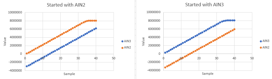
channel1: P: AIN2 N: VCOM
channel2: P: AIN3 N: VCOM

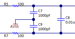
All input signals are given by voltage dividers which are connected to AVDD and AVSS. Therfore each input is close to (AVDD - AVSS)/2. REFP = AVDD, REFN = AVSS. Data is read whenever the nDRDY signal gets low. I tried different Samplerates and a different number of coversions after I switched the mux. There is always the following result:

One of the channels provides a plausible conversion result much faster than the other channel. Lets say I switch the mux and do 10 conversions. Channel 1 delivers a plausible result. I switch to channel 2 and do 10 conversions, the result is 2/3 of what i would expect. If I do 20 conversions after the switching, both channels deliver a plausible result.

If I start my measurement sequence with a different channel, the behaviour swaps. Therefore it is not a problem with the external circuit. All timings and transfered data is the same for both channels. I also analyzed the communication on the SPI Bus level using a logic analyzer to be sure there is no problem.

Is there anyone who can explain the behaviour or who can tell me if the used approach is wrong.

  • Hi Tobias,

    Welcome to the E2E forum! I apologize for the delayed response. This sounds like it could be an issue related to analog settling of the inputs. If your resistor divider resistance values are large and if you have capacitance in the signal path, you may see analog settling. Can you send me your schematic, register settings that you are using, and the data that you are seeing?

    Best regards,

    Bob B

  • Hi Tobias,

    Have you resolved your issues?  Is further assistance needed?

    Best regards,

    Bob B

  • Hello Bob,

    I'm sorry, I didn't recognized your last reply (maybe I missed the update mail). The input filtering is equal to the ADS1261EVM Board.

    Each channel is connected to a resistor divider build from two 350 Ohm stain gauges. What I don't understand is, if it is caused by anaolog settlings, why do I only see the effect on one of the channels? Both channels are build equally  and have the same timing. The only difference is which one was measured first. Unfortunately I currently don't have access to the prototype but I will try to provide the data as soon as possible.

    Thank you very much for your help and patience.

    Best
    Tobias

  • Hi Tobias,

    I need to know the register settings you are using and the exact input configuration.  In particular I would like to know how you are supplying the excitation to the voltage divider and what reference you are using?

    Do I understand correctly that you are using two strain gauges in series?  Or do you have two separate resistor dividers, and if so what is the fixed value of the resistor divider?

    Best regards,

    Bob B

  • Hello Bob,

    the current prototype is based on the ADS1261 EVK hence most of the circuitry is identical to the EVK. The Analog part is powered by the TPS7A4700. There is no external Reference. The ADS1261 as well as the bridges are powered from the 5V analog supply. The following register settings are used:

    Positive Reference is set to AVDD
    Negative Reference is set to AVSS
    -->REF = 0x15
    Samplerate is set to 14400
    Filter is set to SINC4 (should not be relevant for this baudrate --> SINC5)
    --> MODE0 = 0x6B
    Gain is set to 32
    --> PGA = 0x05

    Dependent on the input channel:
    INPMUX=0x3F --> P=AIN2 N=VCOM
    INPMUX=0x4F --> P=AIN3 N=VCOM

    Conversions are started using the START command. All other registers are in reset state. I sketched the input to the ADS1261. Both channels are symmetrical. Only AIN2 and AIN3 are used. Inputs to AINCOM and AIN0/1 can be ignored. The voltage dividers are built from strain gauges. They do NOT build a Wheatstone bridge.

    Captured data with the given settings:

    There is a different behaviour of the symmetrical channels. One of the channels starts negative and is not able to settle within the 40 taken samples. The other channel settles after appr. 35 samples. The behaviour can be moved via software from one channel to the other (dependent on which one was measured first). If both channels are measured correctly, the input voltage is measured as 8030800 (AIN2) and 8039358 (AIN3). The measurement timing is the same on both channels. One measurement cycle on a channel takes 3.163ms. A DMA transfer is triggered via the "Data Ready" signal in order to read the value.

    Thank you very much.

    Best

    Tobias

  • Hi Tobias,

    The drawing did not come through.  Save the drawing as a picture then attach.  I think part of the problem may be the use of VCOM as an input.  I would highly recommend not using VCOM in the measurement but instead use the 2.5V reference output of the ADS1261. VREFOUT can be connected to one of the other analog inputs.  You can repeat the measurement with the mux settings to use the input channel for the REFOUT connection.

    I may have further or possibly a better suggestion based on how the input is being connected and measured.  Initially the comment was made that the input should be near 0.  However, based on the data the converted value settles near full-scale.  You also made a comment about viewing the communication with a logic analyzer.  Can you provide this data?

    Thanks,

    Bob B

  • Hello Bob,

    we used the internal reference (REFOUT connected to AINCOM) in the first place but decided to switch to VCOM in order to have a ratiometric measurement. We didn't do a lot of testing with this configuration, hence we assumed the behaviour of  VCOM is the same for the other inputs as well. You are absolutely right about VCOM. I added a fixed resistor divider to AIN0 and used it instead of VCOM. Already the first conversion can now be seen as settled. This is the behaviour which I expected. Do you have any details why the usage of VCOM is causing the described effects?

    Thank you very much for your help. I would consider the problem as solved. I added the images again as attachment. Let me know if you still need any more data.

    Best

    Tobias

  • Hi Tobias,

    Ok, now I have a better understanding.  Unfortunately I do not have specifics available to me with respect to how the VCOM circuit is implemented.  Generally the resistor values are quite large to limit current in the voltage divider to save power.  Also there is no accuracy specification as to the matching from device to device so your use case would be better served by an external source.  Internally the IC pathways can have considerable resistance and capacitance and when switching from one input to the next there is a differential current due to the input sampling that takes time to settle.  

    Using an external voltage divider should be a much better approach as opposed to using the internal VCOM.

    Best regards,

    Bob B