This thread has been locked.

If you have a related question, please click the "Ask a related question" button in the top right corner. The newly created question will be automatically linked to this question.

ADC12DJ5200RF: ADC12DJ5200RF

Part Number: ADC12DJ5200RF

Hi Team,

We are developing/ designing ADC card using ADC12J5200RF.

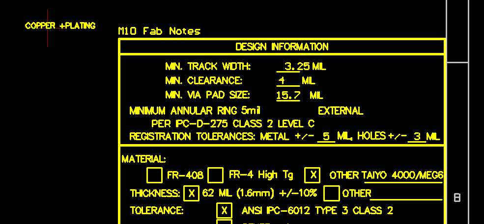
I need some of the following information which is not not available in CAD/GERBER files which is referred from Ti.Kindly do the needful.

1.PCB material and stack-up details?

2.Maximum tolerance between sysref differential clock groups & device clock(Length matching details).

  • Hi Sangeeth,

    All the gerbers and EVM design info can be found here/link on the TI website.

    http://www.ti.com/product/ADC12DJ5200RF/technicaldocuments 

    Simply download the EVM design files, SLVC778.zip.

    There are no distance boundaries needed between the Sysref and Clock traces. Only the differential traces themselves for each. I would keep those under 10mils difference, for each diff pair.

    Regards,

    Rob

  • Hi ,

    Thank you for your quick reply..

    I got all the details except the following,which is i am finding in EVM design files.

    1.Which PCB dielectric material suggest for ADC12DJ5200 for high speed (sampling clock : 5.2GHz) ?,to avoid signal loss.

    2.What is the maximum tolerance do we have to maintain for SYSREF & DEV CLOCK groups.

  • Hi Sangeeth,

    The PCB material is stated in the gerber file download specificed under the fabrication notes, it is Meg6.

    See attached.

    As indicated there is no max tolerance to maintain between the SysRef and Dev Clock groups because all applications will have different layout constraints to work within on their system boards,etc. Timing adjustments to capture the data correctly are made either on the clock signal chain (LMK & LMX parts on the EVM) and/or in the FPGA. 

    Regards,

    Rob