This thread has been locked.

If you have a related question, please click the "Ask a related question" button in the top right corner. The newly created question will be automatically linked to this question.

ADS114S08: External Reference Settings

Part Number: ADS114S08

Hello,

I was given a ADS114S08 that uses an external 2.5V connected to REFP0, which i figured is redundant since it already has an internal reference. A new application rose up, and I switched out the external reverence for one that supplies 3V. When testing the ADC by applying external voltages to the input, i get about a 0.5V offset from what I am applying. 

I'm wondering if the ADC is still using the 2.5V reference. Is the ADC defaulted to using the internal reference? Is there an extra step I missed when using an external reference? Any assistance would be appreciated.

Best Regards,

Miguel Partida

  • Hi Miguel,

    The default power-up configuration is to use the REF0 input pair and the internal reference powered down.  If initially the 2.5V reference was swapped with 3V, then output code will be relative to 3V.

    • Do you have a schematic? 
    • Can you tell me what voltage is being applied to the inputs? 
    • Which analog inputs are you using? 
    • What is the output code you are seeing for the applied input voltage?
    • Can you tell me the register settings you are using?
    • Do you happen to be using the ADS114S08EVM?

    Best regards,

    Bob B

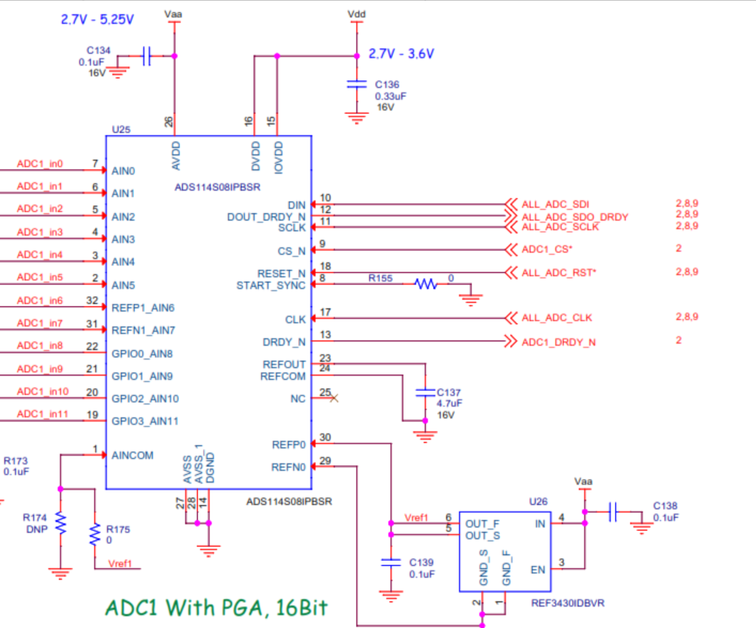
  • I uploaded a schematic, where Vdd is 3.3V and Vaa is 4V.

    I am applying three voltage inputs on

    ADC1_CH6 of 2.5V but seeing 2.08V

    ADC1_CH7 of 4V but seeing 3.326V

    ADC1_CH9 of 2.2V but seeing 1.832V.

    Current register SDI

    REF 0000 0000

    DATARATE 0011 0100

    PGA 0000 100

    INPMUX 0000 1100

    And I am not using the EVM for this application. Let me know if you have any further questions.

  • Hi Miguel,

    I really need to see the output code from the ADS114S08 and not the converted to voltage value as there may be some calculation issue that is unseen.

    There are a couple of issues I see with the schematic.  First, there is a requirement for at least a 330nF cap from AVDD to AVSS.  Second, it is difficult to tell from the schematic, but REFN0 cannot float and should be tied to AGND (AVSS).

    How are you connecting your external voltage source and in particular where does the (-) lead connect?

    Your register settings show you are using AIN0 and AINCOM.  AINCOM is connected to 3V and the AVDD supply is 4V.  So what is connected to AIN0?  Depending on your input selection, based on the schematic relative to AINCOM I would not expect a positive output code for the 2.5V input or the 2.2V input.  For the PGA setting you are missing a digit, but I will assume that PGA bypassed and disabled is the configuration being used.

    So when using AINCOM set to 3V and AVDD at 4V, your input measurement range is 1V positive and 3V negative as your measurement is referred to AINCOM.

    Best regards,

    Bob B