


Other Parts Discussed in Thread: MSP430FR2433,
Hi I have an ADS1231 connected to an MSP430FR2433 in a circuit that is similar if not identical to the reference design.
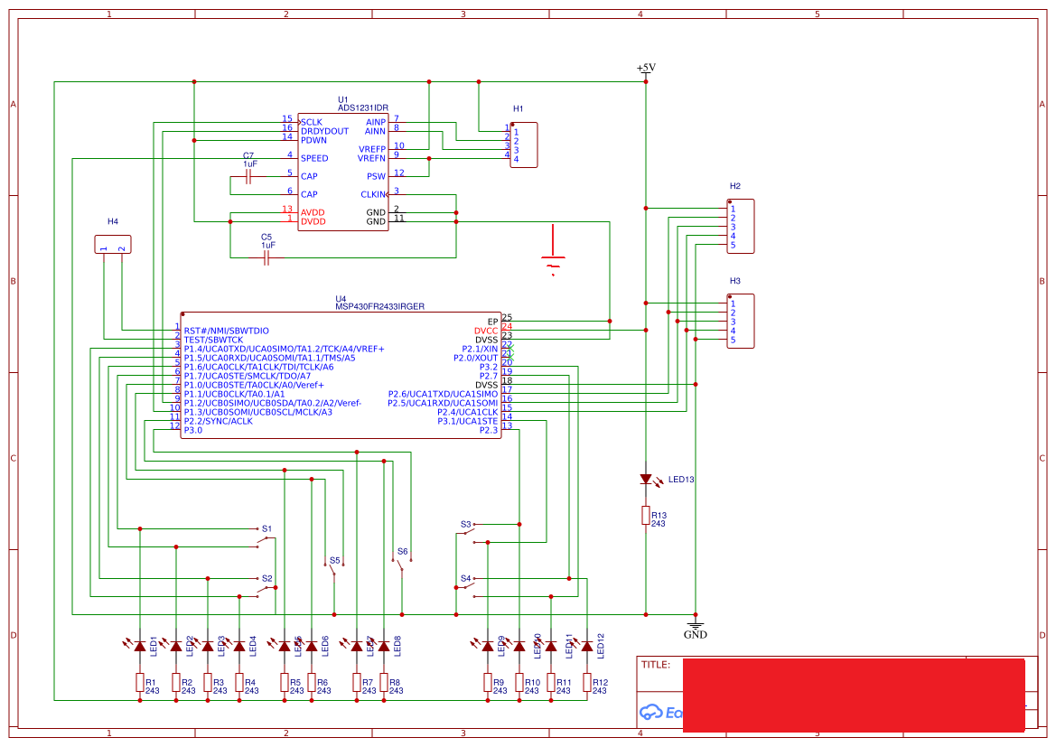
Essentially I have a load cell connected to the ADS1231 which feeds to an MSP430. There are also some switches and LEDs at the bottom which you can ignore.
As you can see, the data rate is set to the slower 10Hz rate. I'm using the internal clock.
I have SCLK feeding to and output on the MSP430, and DRDY/DOUT to an input.
This is all on a 2 layer PCB. The two chips are 10 mm apart.
Power is USB via a Launchpad @ 3.3V.
Here are my problems.
- When the MCU is setting SCLK high or low, I can see nothing on my scope. I can only assume it is a low impedance pin that is sinking my signal.
- The output at DRDY/DOUT is strange. Under some conditions it is normal. If SCLK is held LOW, DRDY is HIGH.
- However if I try to read data, DOUT is giving me strange output. Take a look at this plot:

In my program in the MCU, I wait for DRDY to go low. When it does I blip an unrelated output which is the blue line that you see. Note that this pulse is about 1ms@3.3V.
Then I set SCLK HIGH, wait 1ms, read DOUT, set SCLK LOW, etc. and repeat for the next 23 (+1) bits.
However the yellow waveform that you are seein at DOUT is really simply reflecting SCLK, except note that it is only ~1.4V. That is invalid since the datasheet says that LOW should be MAX 0.66V and HIGH should be minimum 2.9V, given 3.3V in.
You can also see that I get some 3.3V spikes kind of erratically; which does not seem to relate to anything.
The program reflects what I just described:
#include <Arduino.h>

#define DOUT P1_3
#define CLK P1_2
#define PULSE_WIDTH 1000

uint16_t in[3];
void pause(void);
uint8_t SPI_transfer_byte(uint8_t);

void setup() {
  Serial1.begin(9600);
  pinMode(6, OUTPUT);
  pinMode(CLK, OUTPUT);
  pinMode(DOUT, INPUT);

  // Reset DOUT with a pulse.
  digitalWrite(CLK, HIGH);
  pause();
  digitalWrite(CLK, LOW);
  pause();
}

void loop()
{
  if(digitalRead(DOUT) == LOW)
  {
    // Blip an output to trigger scope.
    digitalWrite(6, HIGH);
    pause();
    digitalWrite(6, LOW);

    for(int i=0; i<3; i++)
      in[i] = SPI_transfer_byte(0);
    Serial1.print(in[0], HEX);
    Serial1.print(in[1], HEX);
    Serial1.print(in[2], HEX);

    // Reset DOUT with a 25th pulse.
    pause();
    digitalWrite(CLK, HIGH);
    pause();
    digitalWrite(CLK, LOW);
  }
  Serial1.write(".");
}

uint8_t SPI_transfer_byte(uint8_t byte_out)
{
    uint8_t byte_in = 0;
    uint8_t bit;

    for (bit = 0x80; bit; bit >>= 1)
    {
        pause();
        digitalWrite(CLK, HIGH);
        if (digitalRead(DOUT) == HIGH)
            byte_in |= bit;
        pause();
        digitalWrite(CLK, LOW);
    }

    return byte_in;
}

void pause()
{
  delayMicroseconds(PULSE_WIDTH);
}
I have tried:
- Connecting or not connecting a load cell.
- Changing the pulse width. The datasheet says I should be reading 24 bits in less than 100ms.
- A different PCB with different chips in case of damage or faulty PCB.
- Double checking the reference designs against my schematic and PCB layout.
This is the PCB


Thanks in advance.

