This thread has been locked.

If you have a related question, please click the "Ask a related question" button in the top right corner. The newly created question will be automatically linked to this question.

DAC161S997: SPI communication issue, device no feedback

Part Number: DAC161S997
Other Parts Discussed in Thread: LM2841,

Dear Sir :

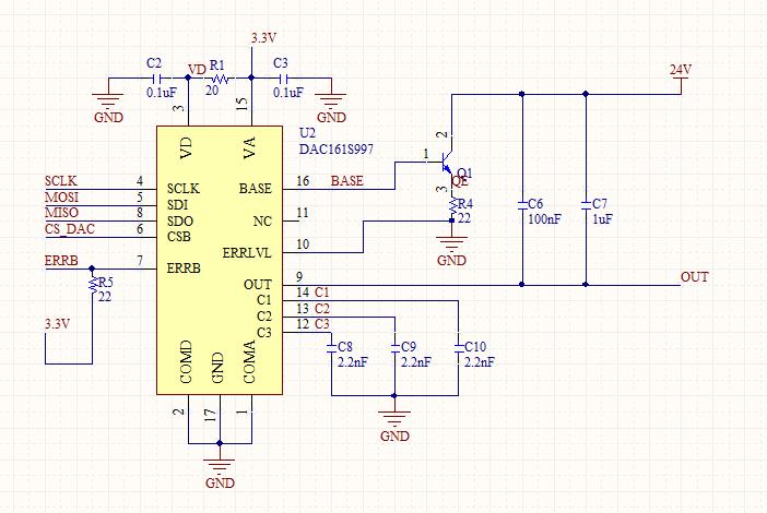
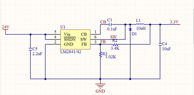
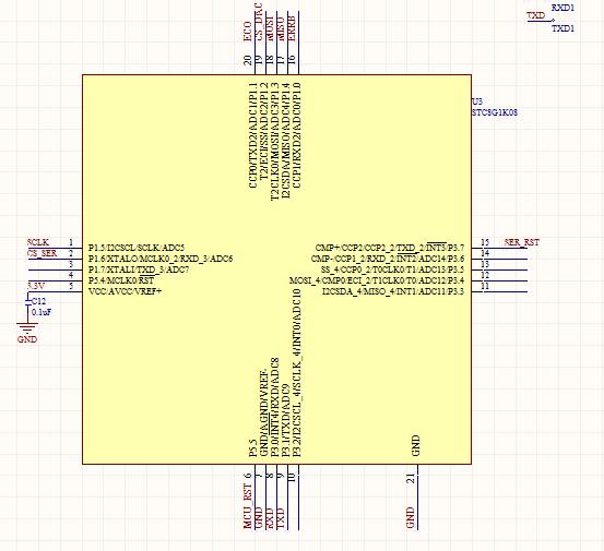
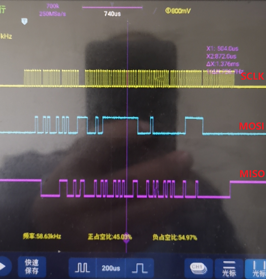
            I plan use DAC161S997 , transfer SPI data to 4-20mA output , i almost use typical application circle . just change LDO to switch power LM2841. now i can communicated with MCU with Uart, but i can't get the right answer from DAC, when i send command to DAC . i use simulate SPI function . the code as below , pls.   help me review it , very appreciate if you can give me some suggestion.

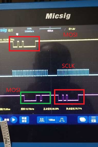
            when i run test () , only get "FF" ,"FF","FF" from DAC . 

/* read 1 bit from SPI. return data */
u8 SpiReadByte(void)
{
u8 i,rByte=0;
SCLK=0;
for(i=0;i<8;i++)
{

SCLK=1;
rByte<<=1;
rByte|=MISO;
SCLK=0;


}
return rByte;
}
/*SPI send 1 bit */
void SpiSendByte(u8 dt)

{
u8 i;
for(i=0;i<8;i++)
{
SCLK=0;
if((dt<<i)&0x80)
MOSI=1;
else
{
MOSI=0;
}
SCLK=1;
}
SCLK=0;

}

Void test ()
{
u8 outData[3], i;
CS_DAC = 0;
outData[0] = 0x04;
outData[1] = Data >> 8;
outData[2] = Data & 0xff;

for (i=0; i<3; i++)
{
SpiSendByte (outData[i]);
Delay_ms(20);
}
Delay_ms(2);
SpiSendByte(0x89);
w[0]=SpiReadByte();
SpiSendByte(0xff);
w[1]=SpiReadByte();
SpiSendByte(0xff);
w[2]=SpiReadByte();
CS_DAC = 1

}

  • Hello Jeffrey,

    I would first recommend you to confirm the correct startup of the loop by checking the supply voltages VD & VA, the output voltage of the switcher LM2841 and the initial loop current after power up. If the loop starts up correctly, then proceed with testing your function test(). I have a couple of comments about your code.

    1. It seems your code is intended to write data: 0x08FF to addr:0x04 (data register) however you're reading back from addr:0x09? Is that correct? contents of addr 0x09 depend on the status of the chip and if there are loop and SPI errors, the output could be 0xFFFF

    2. Reading data from the registers requires two commands. The first command is to initiate the read operation and the second  should be a NOOP command to clock out the contents of the register. It looks like you're missing the NOOP command in your test() method

    3. Can you connect your SPI signals to an oscilloscope and share a screenshot of the waveforms?

    Regards,

    Reza

  • Dear Reza :

                 Very appreciate you response me so quickly . still need you professional support here .

                so far , I believe , DAC have powered up , because we can get SCLK signal and MISO signal of DAC on oscilloscope 。 but feedback value still incorrect .

                we send address + data to DAC , but get same feedback .

                for example  :  send 0x89 0x05 0xff      DAC feedback : 0x89 0x05 0xff      (0x09 is address of DAC register status , in general , feedback should be 0xeX , X maybe other numbers )

                                        send 0x89 0xff 0xff       DAC feedback : 0x89 0xff 0xff     

                would you do me a favor give me some advice how to edit read ( ) and write () ?  or what's format or template of read () and write() ? so far, I use GPIO simulate SPI .

                BTW, we find ERRB was pull low , on schematic, it attached to VSS .  attached my schematic below .

     thanks !      

    1. It seems your code is intended to write data: 0x08FF to addr:0x04 (data register) however you're reading back from addr:0x89? Is that correct? contents of addr 0x89 depend on the status of the chip and if there are loop and SPI errors, the output could be 0xFFFF

    Jeffrey Answer :  because we want to realize two step :  1 : write date to 0X04 ; 2 : read status date from 0X09  .

    2. Reading data from the registers requires two commands. The first command is to initiate the read operation and the second  should be a NOOP command to clock out the contents of the register. It looks like you're missing the NOOP command in your test() method

    Jeffrey answer : would you do me a favor give us some clear advice how to write read() function . we try it again and again , but still can't get right feedback .  

    3. Can you connect your SPI signals to an oscilloscope and share a screenshot of the waveforms?

    Jeffrey Answer : sorry for some reason , we can't get waveforms screenshot now . we just capture them with different Picture .


  • Dear Reza :

                  pls. check snapshot of oscillator  , according to picture , after send command + data 8900ff (in red box ) to DAC , then, we get feedback from it , but we found 2 groups datas (in green box and red box), I can't know which one is right .  

                 if you check wave in red box carefully , they are same , it mean we read back what we send . just try 8900ff , no specific objective .

                so far, we just assume as below .( we used SPI model 0)

    1. MCU send data to DAC

    2.DAC response , but value incorrect .

            so , my question is .

            1. what format should I follow when send or read data from DAC ?

            2. what data show DAC work ?

            3. what can I do next ?

  • Hello Jeffrey,

    Your SpiReadByte() and  SpiSendByte(dt) functions look fine to me. By default, the SPI shift register always outputs the previous SPI Write frame on the SDO line. This is the reason why when you send  0x89 0xff 0xff, you readback  0x89 0xff 0xff from the SDO line. 

    To read back a register correctly, you have to follow the read command with a NOOP command. An example is below.

    Send 0x89 0xFF 0xFF (read command addr 0x09)

    Send 0x00 0x00 0x00 (NOOP command). Read back SDO bits during this frame. 

    I will modify the test code as shown below.

    **************************************************************

    Void test ()
    {
    u8 outData[3], i;
    CS_DAC = 0;
    outData[0] = 0x04;
    outData[1] = Data >> 8;
    outData[2] = Data & 0xff;

    for (i=0; i<3; i++)  // Send 0x0408FF 
    {
    SpiSendByte (outData[i]);
    Delay_ms(20);
    }

    CS_DAC = 1;

    Delay_ms(2);

    // Send Read Cmd for addr 0x09

    CS_DAC = 0;
    SpiSendByte(0x89);
    SpiSendByte(0xff);
    SpiSendByte(0xff);
    CS_DAC = 1

    Delay_ms(2);

    // Send NOOP command. Read SDO during this frame

    CS_DAC = 0;

    SpiSendByte(0x02);
    w[0]=SpiReadByte();
    SpiSendByte(0x00);
    w[1]=SpiReadByte();
    SpiSendByte(0x00);
    w[2]=SpiReadByte();
    CS_DAC = 1

    }

    Two more things to note.

    1. SDO data is clocked out on the falling edge of SCLK. You may have to change the polarity of SCLK in the read() function to clock out data correctly. This would be easier to observe on an oscilloscope though. 

    2. Between the falling edge and rising edge of CS, there should be integer multiples of 24 SCLKs. If there is a non-integer multiple number of SCLKs, the SPI frame is discarded and an error is reported.

    Regards,

    Reza

    Regards,

    Reza


  • Dear Reza :

                  thank your information .

                 I update my function follow your instruction , seems output still not meet our original expectation . new function as below .

               for example :

                           send (0X89) ; send(0XFF)   ; send(0XFF) ;

                           send(0x02); read(); send(0x00); read(); send(0x00); read();

                           we got result: 000200 ;

                       if send other numbers

                           send(0x08); read(); send(0x06); read(); send(0x04); read(); // 08,06,04 no meaning , just easy for check resulting, but seems it still work , have value return .

                           we got result 000806, seem we read same data that we send out and add 00 at high bits.

                in addition , we send data to DACCODE register  , but loop current output value incorrect ,even over 24mA . because I can't read register status (can't get right return) , so I don't know actual reason . (in order to avoid static power consume affect , I have removed DCDC LM2841 from circuit , offer 3.3VDC to DAC and MCU directly , 24VDC contact with triode as loop+ ,almost like 4-wire loop current  )

                for example , we send (2AAA) to 0x04 , ideal loop current should be 0mA , but measurement current is 5.2 mA . other test results as below , I can’t find regularity between them.

    input value

    ideal current

    loop current out

    2AAA (0%)

    10922

    4

    5.2

    5554(25%)

    21844

    8

    10.27

    7FFF(50%)

    32767

    12

    15.37

    AAAA(75%)

    43690

    16

    20.48

    D555(100%)

    54613

    20

    25.54


    My suspection :

             My send() and read() words format in test() still have some problem ,maybe other issue, so I can’t get right feedback . at same time,  we can get SCLK,MISO,MOSI signals on oscillator , although I don’t know feedback value right or not .

    Need support :

    1. would you help you check test() ,what; s wrong in it ? what’s right template of send() and read() ? I can’t find these information on datasheet .

    2. what’s feedback show DAC good running ? like read(0x89) , get result : E0 or other method .

    Btw : why do we send 0x02 ? can we use other number ? such as 00,03,04 etc.


    void Test (u16 Data)
    {
    u8 outData[3], i;
    CS_DAC = 0;
    outData[0] = 0x04;
    outData[1] = 0x2a;
    outData[2] = 0xaa;
    for (i=0; i<3; i++) // Send 0x042aaa
    {
    SpiSendByte (outData[i]);
    Delay_us(10);
    }
    CS_DAC = 1;
    Delay_us(30);  // in order to show all waveform on oscillator , we change delay time
    // Send Read Cmd for addr 0x09
    CS_DAC = 0;
    SpiSendByte(0x89);
    SpiSendByte(0xff);
    SpiSendByte(0xff);
    CS_DAC = 1;
    Delay_us(10);  // in order to show all waveform on oscillator , we change delay time 
    // Send NOOP command. Read SDO during this frame
    CS_DAC = 0;
    SpiSendByte(0x02);
    w[0]=SpiReadByte();
    SpiSendByte(0x00);
    w[1]=SpiReadByte();
    SpiSendByte(0x00);
    w[2]=SpiReadByte();
    CS_DAC = 1;
    }

    /*read a bit from SPI, return data*/
    u8 SpiReadByte(void){u8 i,rByte=0;SCLK=0;for(i=0;i<8;i++){SCLK=1;Delay_us(5);;rByte<<=1;rByte|=MISO;SCLK=0;Delay_us(5);} return rByte;}
    /*SPI send 1 bit*/
    void SpiSendByte(u8 dt){u8 i;for(i=0;i<8;i++){SCLK=0;Delay_us(5);if((dt<<<i)&0x80)MOSI=1;else{MOSI=0;}SCLK=1;Delay_us(5);}SCLK=0;}

    have a good weekend !

    thanks a lot !

    Best regard

    Jeffrey

     // in order to show all waveform on oscillator , we change delay time

  • Hello Jeffrey,

    I'm glad that you've made some progress on this and with the additional info, we can figure this out. I suspect the issue you have is with the test function. Remember that it is critical to always have integer multiples of 24 SCLKs to communicate with the DAC. If this is not done, the contents of the shift register can get distorted. The way the read() method is used currently will cause a shift in the contents of the SPI shift register. My suggestion is to define new functions that ensure that all DAC SPI read & write operations have only 24 SCLKs. See below

    I took another look at your functions for SpiSendByte(dt) & SpiReadByte() and we can modify them slightly to achieve the purpose. First, I'll combine the two functions into a single one.

    ****************Generic SPI Byte function that Writes on Rising SCLK edge and Reads SDO on Falling edge****************************

    /*Generic WR RD SPI Byte*/
    u8 SpiSendByte(u8 dt)


    u8 i, rByte=0;
    for(i=0;i<8;i++)
    {
    SCLK=0;
    if((dt<<i)&0x80)
    MOSI=1;
    else
    {
    MOSI=0;
    }
    SCLK=1;

    SCLK=0;

    rByte<<=1;
    rByte |=MISO;
    }

    return rByte;
    }

    ***********************Define 24 bit WR/ RD Function*****************************************************************

    u32 dacWR (u8 addr, u8 hiByte, u8 loByte)
    {

    u8 a, b, c = 0
    u32 data = 0;
    CS_DAC = 0;

    a = SpiSendByte (addr);
    Delay_ms(20);

    b = SpiSendByte (hiByte);
    Delay_ms(20);

    c = SpiSendByte (loByte);
    Delay_ms(20);

    CS_DAC= 1;
    data = a<<16 + b<<8 + c;
    return data;

    }

    ***********************Test Function.  Modify delays as necessary*****************************************************************

    Void test ()
    {

    u32 dummy, SDO = 0;

    CS_DAC = 0;

    dummy = dacWR(0x04, 0x08, 0xFF);  // Write to Data register (0x0408FF)                                                                                                                                                                                                                                Delay_ms(20);
    dummy = dacWR(0x89, 0x00, 0x00);  //Send RD command for addr 0x09                                                                                                                                                             Delay_ms(20);
    SDO = dacWR(0x02, 0x00, 0x00);  // Send NOOP command to clock out SDO bits

    CS_DAC = 1;

    }

    A good way to ensure correct operation of the DAC is to read back the status register (addr 0x09). The read back data should be E0, just like you mentioned. Please not that you have to either continuously (default of every 100ms) send valid SPI data to the chip to avoid a SPI timeout error or you'll have to mask the error bit in the ERR CONFIG register (addr 0x05).

    Also for reading back data, you can use any SPI address but I suggested addr 0x02 because it is the NOOP command and it doesn't carry out any specific command.

    One more thing you can do is to read back the SDO bits for every 24bit SPI write operation. By default, the SDO bits will always be the same as the previous 24bit SPI frame. You can use this to verify the correct SPI write and read operation of the chip.

    Let me know if this resolves the issues. Thanks.

    Regards,

    Reza


  • HI Reza :

                 thanks your suggestion , I will try and reply result to you when complete.  

                 I found another issue about NPN transistor, it very high temperature when I add 24VDC on loop +. is it affect DAC run and output? how can I reduce heat that generates from it? 

                 I found additional 100 Ω resistor and Zener diodes used in schematic before NPN transistor (on the datasheet Page 26). what's the function of them ? can I add them into my circuit?

                 have a good day! 

    thanks

    Jeffrey 

    Best Regard 

  • Hello Jeffrey,

    The zener diode is used to ensure that when the loop supply voltage is low, the input voltage used for the LDO is still sufficient to generate 3.3V VCC for the example provided. For this example, a 3.9V zener is used to guarantee a well functioning LDO under all loop supply and current conditions. The 100ohm resistor can also be added in series with the zener.

    The NPN transistor is heating up in your example because most of the output power is dissipated on the BJT (appox 24V * loop current). Using the series combination of the zener diode and 100 ohm resistor will help reduce the heat dissipation on the BJT. Please ensure that the BJT is rated properly and has a beta = 40 minimum and Vceo = 40V minimum.

    Regards,

    Reza

  • Dear Reza :

                 I updated code with you suggestion , now , we can communicated with DAC and got feedback "E0" from 0x09, i believe DAC worked now . now we faced an accuracy issue , When i give D555 to DAC from serial port,  it gave back 19.9mA at begining , but it slowly drop down to 19.5mA , i suspect ,NPN heat (when 20mA and 24V make it high temperature )make output drift . so i try to reduce heat from NPN. 

                About existing Zener diode and resistor that use in schematic , how much voltage can they reduce ? how to calculate drop voltage ?   Can i change 100Ω to more , like 500 Ω or 1K Ω , consume more power , make less voltage imposed on NPN ?  I tried add 12V on loop + , NPN's temperature is ok for me . 

                Keep safe in this special time period. 

    thanks !

    Jeffrey 


  • Hello Jeffrey,

    I'm glad the SPI now works properly.

    It is possible that the heating of the NPN causes a drop in its beta and this results in reduced accuracy for the loop. The best way to confirm that is to check the current accuracy with a lower supply voltage or with some series resistive load to the loop+, loop- terminals. 

    The zener diode used in the application circuit is a 3.9V zener and will reduce the voltage across the NPN by approx 3.9V. The 100ohm resistor on the collector (Rc) can be increased so long as the loop compliance voltage requirement is still met. Increasing Rc will also reduce the NPN Vce voltage. Increasing Rc

    Loop compliance voltage determines what the minimum loop supply voltage can be. Using KVL, under max I_loop conditions, the sum of all voltage drops across the loop components should be less than the minimum loop supply. This is explained in section 9.2.2.2. of the datasheet. From equation 22 under that section, the minimum loop supply is determined to be 9.3V when Rc = 100ohm and Rload(max) = 250ohm.

    Increasing Rc means that the minimum loop supply needs to increase by 24mA*Δ Rc or the max Rload reduces by ΔRc.

    I hope that helps.

    Regards,

    Reza

  • Dear Reza : 

                Yes, you are right, the temperature in acceptable range if used low voltage (like 12VDC) or small current (4mA ) .consider whole system accuracy,i need control all device 's temperature less than 35°C.  

               if "The zener diode used in the application circuit is a 3.9V zener and will reduce the voltage across the NPN by approx 3.9V " , Can i use one Zener diode with high voltage, such as 6V or 8V?  then it will consume more power ? but i don't know what others impact if change this Zener diode voltage ? after all, it's original function to make sure LDO sufficiently offer 3.3V . (Now , i use one DCDC instead of LDO)

              Rload should less than 250 ohm and loop voltage is 24VDV, more than 9.3V, so i will try to increase Rc to 500 or 1K first. i am trying reduce heat of whole system from all points. very appreciate if you have any advice to reduce heat. 

    thanks 

     Jeffrey 

    Best Regard 

  • Hello Jeffrey,

    The 3.9V zener was selected to ensure that the minimum input voltage for the LDO is always satisfied. You can use a 6V or 8V zener as well but you should sure that this value is larger than the miminum input voltage for your selected DCDC. The zener wattage should also be sufficient when I_Loop max = 24mA flows through the zener.

    For your loop supply of 24V, you cannot change Rc to 1kohm since this will violate loop compliance at 24mA. Please follow the guide line below

    Loop Supply > Vzener + I_Loopmax(Rc+ Rload_max) + 4V

     For a 24V supply, 8V zener and 250ohm max load, this limits Rc_max to 250ohm.

    Regards,

    Reza

  • Hello Jeffrey,

    Do you have any updates on this design? If not, can you close this thread and reopen another if a new issue comes up? Thanks!

    Regards,

    Reza

  • HI Reza :

               sure , I will close this thread first . thanks your precious time and professional advice .

    thanks !

    Jeffrey