This thread has been locked.

If you have a related question, please click the "Ask a related question" button in the top right corner. The newly created question will be automatically linked to this question.

ADS8556: Convert range not given expected results

Part Number: ADS8556

Hello,

I've been working on an ADS8556. The goal is to use it in hardware mode with possibility to vary range multiplier between 2x and 4x using the 2.5V internal reference. So our input shall be between -5V to +V5 and -10V to +10V. For communication we set serial mode.

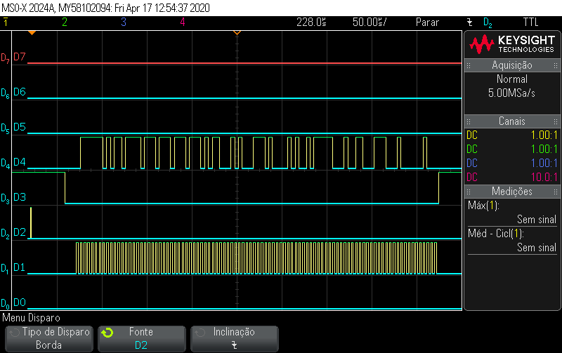
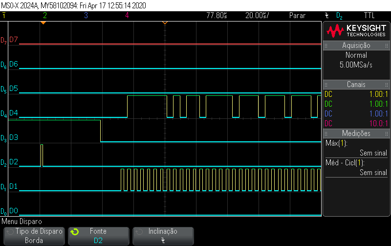
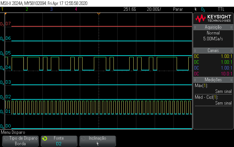
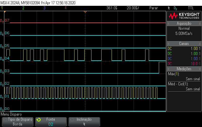
We have build a custom board using an MSP432E40Y and so far I've managed to communicate with the ADS. But I found something wierd, I've set (via hardware) the range to be 4x and to use the internal reference on its default (never programmed in software mode), I read (using a multimeter) 2.5V on pin 51.

This way I shall get the maximum positive number 0111111111111111 (+10V) and minimum negative number 1000000000000000 (-10V), at least according to the table on datasheet.

I'm using a rectified DC power supply to test the analog input against the data I receive digitally. If I set the power supply to +5V around (4.99V) the receive digital data is very close to 0111111111111111 If i go above that I get negative data (overflow on the 16th bit?) If I set the range to be 2.5V I get the same behaviour at the 2.5V. If I set the power supply to -4.99V I get values close to 1000000000000000, if go below (-5.02V) I get positive data (overflow again?) Do we have something wrong with our schematic? Did we forgot something?

ADS8556 Schematic:

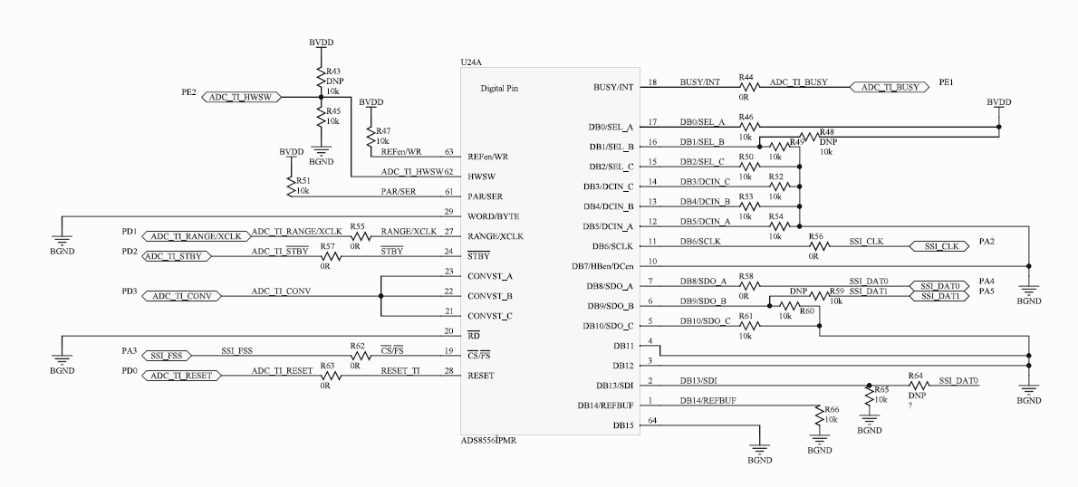
ADC_TI_RANGE/XCLK is controlled using the MSP. Set to 0 by default.

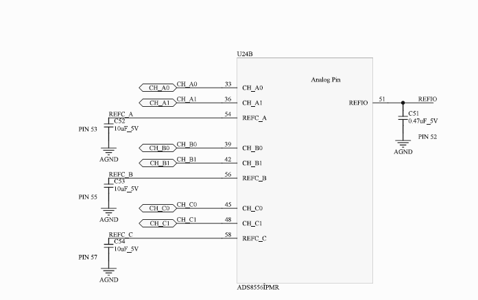
Appreciate any help regarding this question.

Another thing, doing a reset to the ADS also reset the internal registers, or do they hold their values between resets?
Thank you.

  • Hi Andre,

    Your schematic looks good. However, I do have two questions:

    1. Are you connecting AGND and BGND somewhere on the circuit board?
    2. What's your HVDD and HVSS supply voltage? they are not shown in your schematic.

    Other suggestion and requirement:

    First, please check the voltage on pin 27 to make sure it's low and close to 0V, I suggest you to connect this pin to your BGND directly for +/-4Vref range or to BVDD for +/-2Vref input range as a test purpose.

    Second, please provide timing plots of SCLK, BUSY, /CS, and SDOA with different input voltage under hardware mode, a closer timing of one cycle is good and this will be very helpful to address the issue.

    Regarding your question about reset, a pin-controlled reset(RESET) issued on pin 28 will reset control register(CR) content to the default value.

    Thanks&regards,

    Dale

  • Hi Dale,

    Regarding what you've asked for:
     1. Yes, The AGND is connected to all the analog circuitry part and BGND to the digital one. These 2 are connected trough a ferrite choke.
     2. :

    I've removed R55 (1st post diagram) and grounded pin 27 to BGND.
     Got the exact same result (-5V to +5V instead of -10V to +10V).

    Providing communication timings:
    Ch1: SCLK
    Ch2: BUSY
    Ch3: /CS
    Ch4: SDOA

    One complete cycle in one image:

    One complete cycle in multiple images:

    Thank you very much for your help.

  • The 2nd point miss the image. I'm sorry for that. This is the image:

  • Hello Dale,

    I think I found the problem. My SCLK sinal was low during the /FS down, and started low, so I think I was losing the 1st bit of the communication, and get only half the values I should.

    On the positive side, I get the full range or at least very close (9.99984). But As I continue my implementation I got 2 problems.

    1 - Can't get negative numbers (not doing the correct transformation must likely).

    2 - Can't get speeds over 7Mhz, I'm not using SPI, as I can't get it work by any means (IF you have some sort of example on how to use SPI with this ADC I would be really thankfull).

    Thank you.

  • Hi Andre,

    I apologized for missing your update.

    Regarding your questions:

    1. Can you please let me know what code your got? what's your negative input voltage?

    2. Unfortunately, we do not have a sample code released with this ADC. Are you using GPIO to simulate SPI interface on your controller?

    Thanks&regards,

    Dale

  • Hi Dale,

    No problem.
    I end up resolving my issues.
    1. I was not using the correct variable type, the int type on MCU is 32bits and the device response is in 16bits, so the negative values were considered positives (no overflow), the solution was to use short int type(16bits).

    2. Yes I was using the GPIO to simulate the SPI interface, until I realize the limitation on using it directly. In the mean time I understand the SPI initialization of the MSP432E40Y and verified I had the MCU data in missplace (was on PA4 and should be at PA5 on SSI0 configured as lagacy SPI.

    With this alteration the ADC is now able to perform and communicate correctly with the MCU.

    Thank you for your time,

    The problem is solved!

  • Hi Andre,

    Thank you for update, please let me know if you need further support.

    Regards,

    Dale