This thread has been locked.

If you have a related question, please click the "Ask a related question" button in the top right corner. The newly created question will be automatically linked to this question.

DAC81408: No matter what I do with this DAC, I can't get an output.

Part Number: DAC81408
Other Parts Discussed in Thread: USB2ANY, , DAC8718, DAC7734

Hi,

I have been trying to get this DAC work for a month. I even got the evaluation board twice, but not the USB2ANY interface cable. I tried interfacing to the DAC myself using python. I have used other DACs and they work fine.

So here's the issue with the DAC:

1. I see absolutely nothing in the outputs.

2. No SDO is issued.

So this is what I did for the DAC circuit (I'm not suing the evaluation board anymore):

Vcc = 10V

Vss = 0V

Vio = 5V (tried 3.3V and no response)

Vdd/Vaa = 5V

Vref = 5V

I Connect the CLR, RESET and LDAC pins to high (5V) so I don't have to worry about them until I can actually get a simple response from DAC.

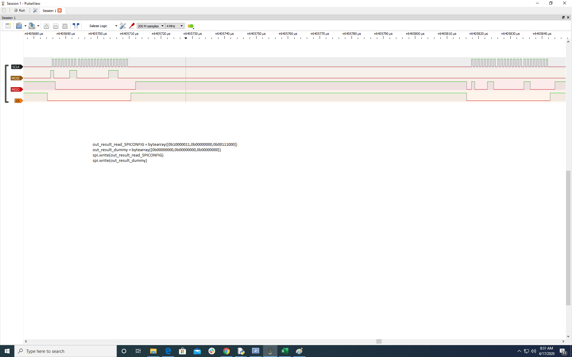
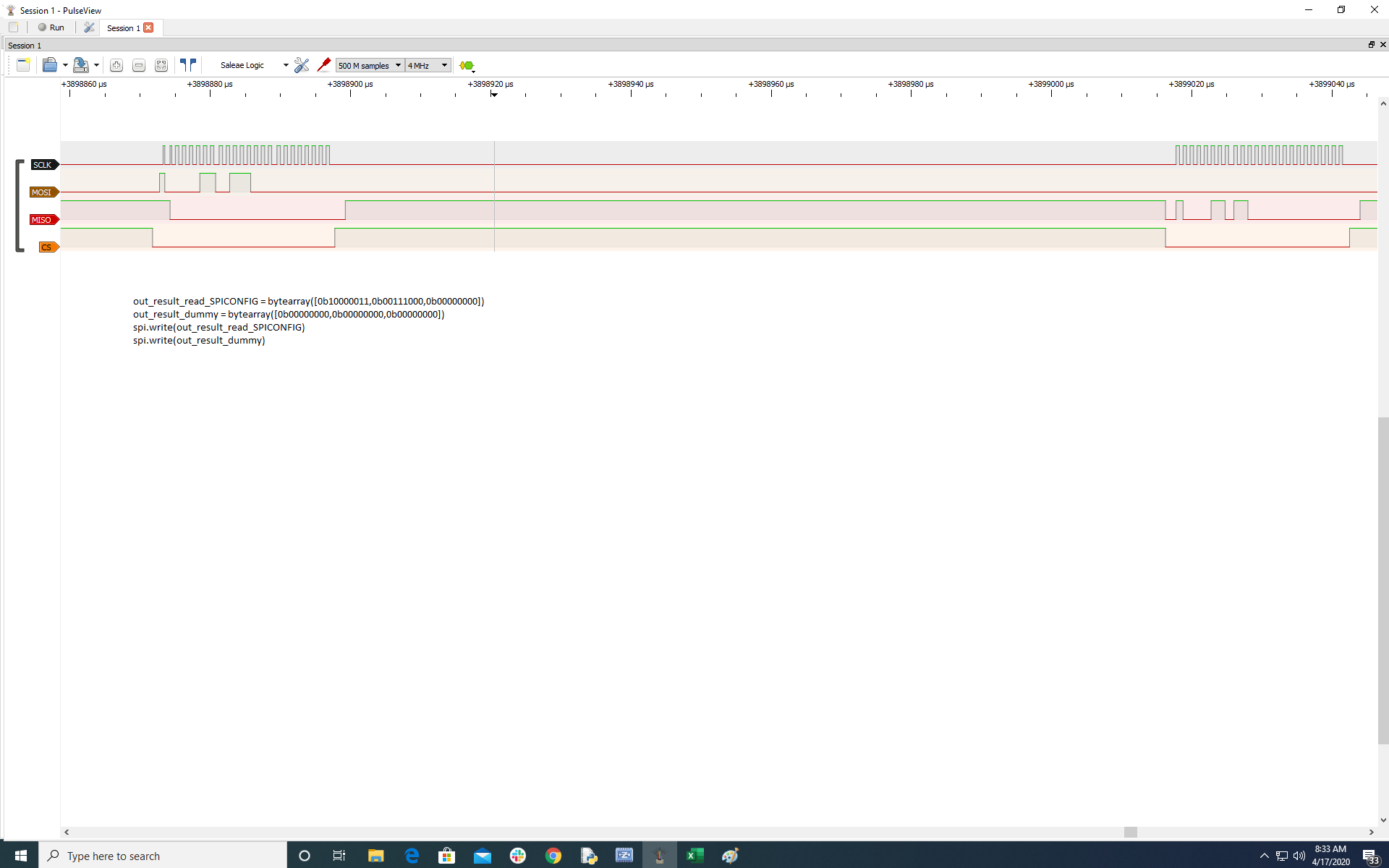
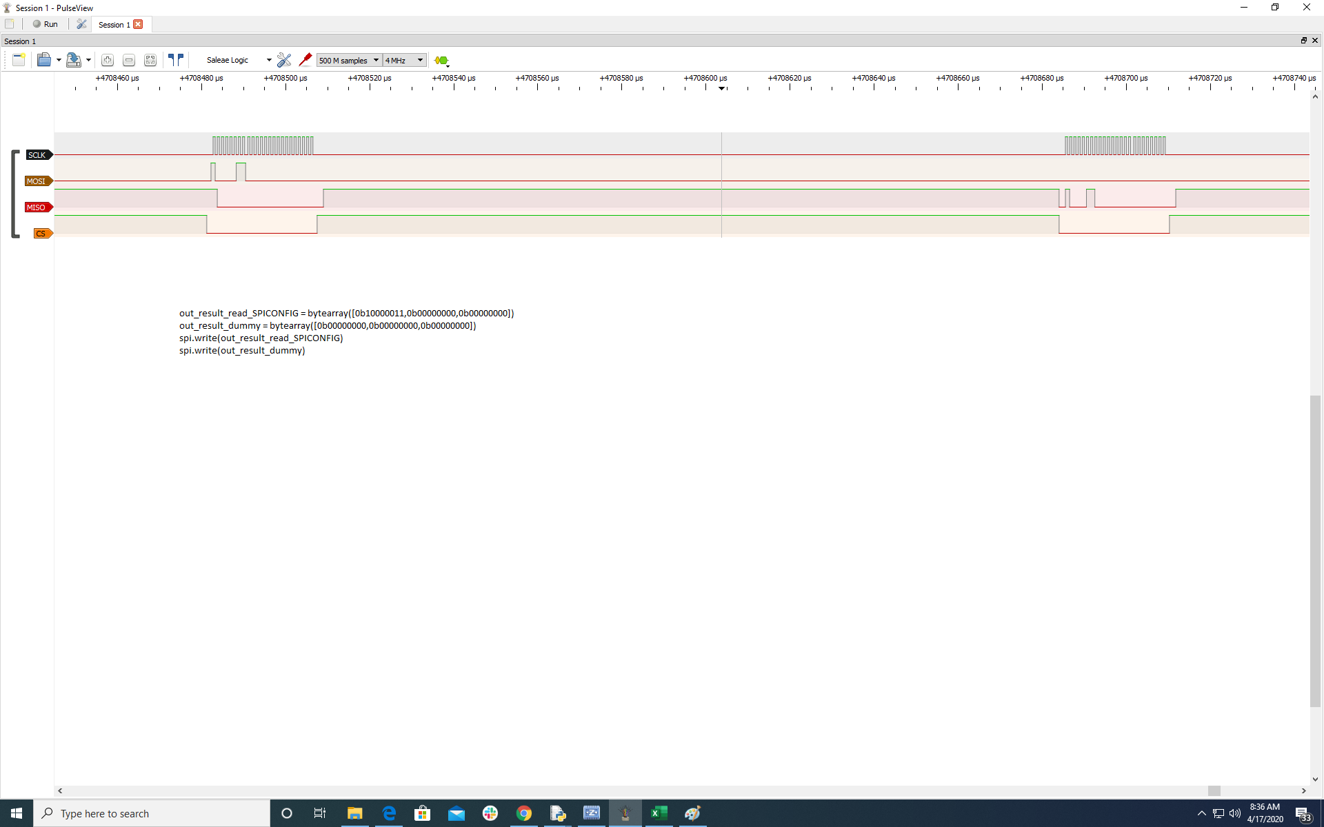
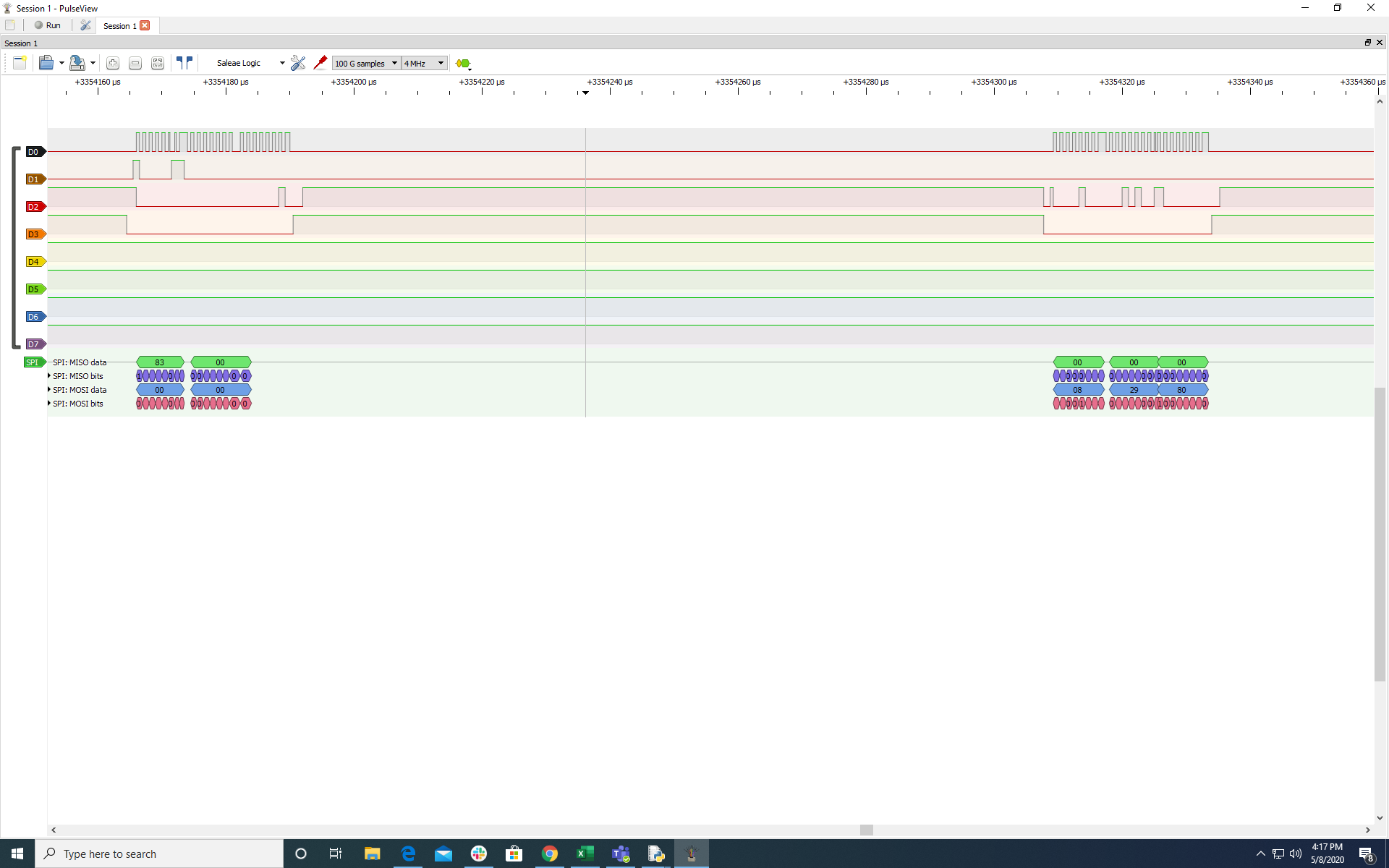
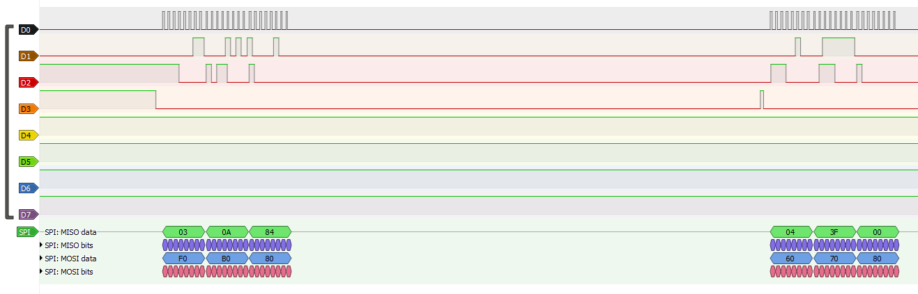
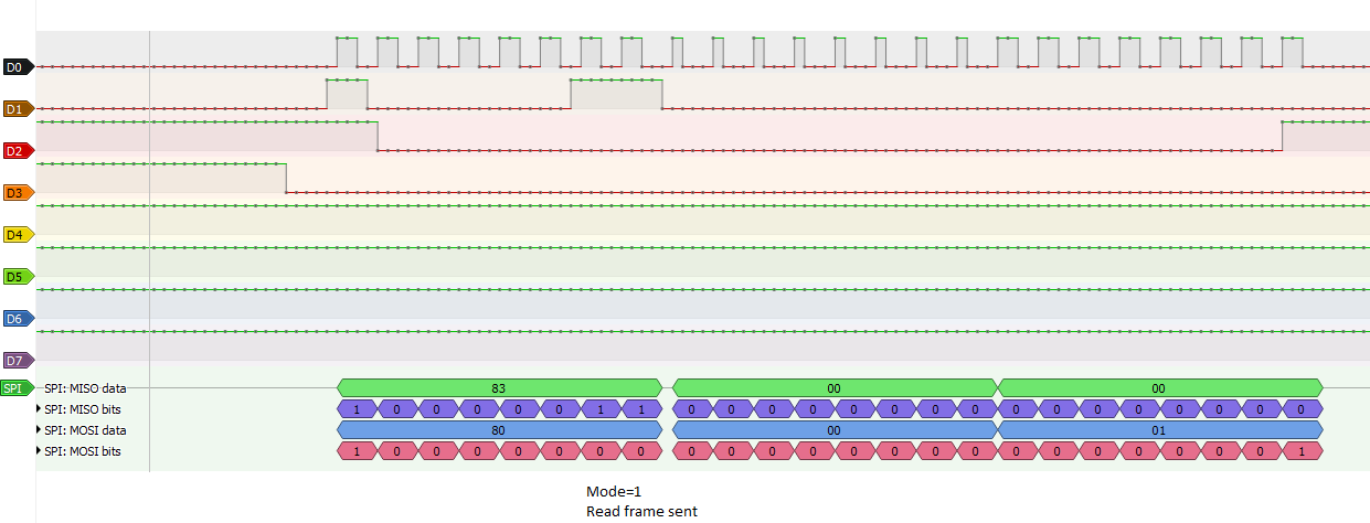
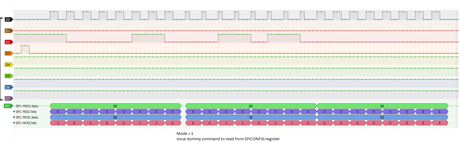
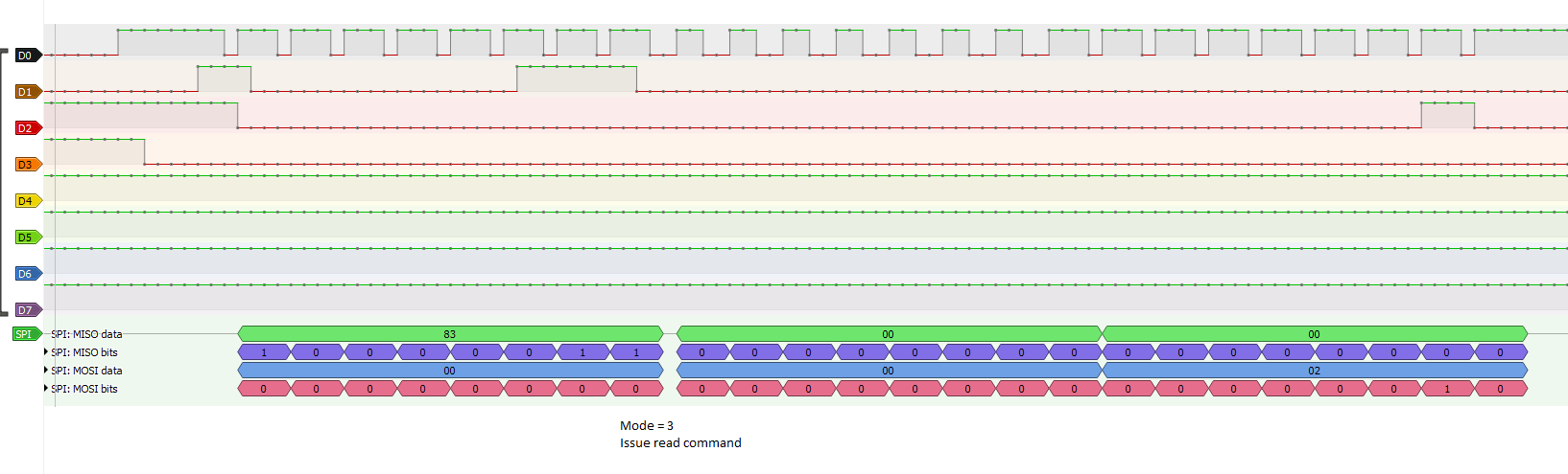
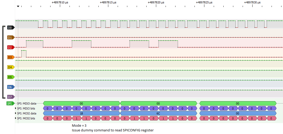
When I try to communicate with the SPI, here's what I do with the registers (obviously CS should go low before writing, no CRC, no LDAC, no broadcast, no toggle, no differential and in asynchronous mode... as simple as possible):

*First byte is to write to a register, and two other bytes are the data (based on DAC datasheet)


Trigger register = 00001110 , 00000000, 00001010 (I want to do soft reboot of the device before changing the registers)

SPI Configuration Register = 00000011, 00000000, 00000100 (I want to enable SDO and also, take the device to active mode)

DAC Power-Down Register = 00001001, 11110000, 00001111 (I activated all the DAC outputs, so no power-down) 

General Configuration Register = 00000100, 01111111, 00000000 (I power-down the internal reference and use a 5V external reference)

And then I try writing to OUT0 ... but nothing.

Can someone please help me? I tried everything with the evaluation board as well to no avail.

Thank you!

  • Hi Afshari,

    First of all you cannot have 5V reference on this. If you read datasheet clearly, its 2.5V.

    Also for writing into device we need 24 SCLK continuously, otherwise it will ignore SPI frame

    To debug this issue, I want you to do the following steps.

    1. Power up the device, so POR event will happen and all registers will be in its default state and DAC is in powered down state, along with internal reference disabled.

    2. By now SDO will be operational since SDO-EN bit will be 1 by default.

    3. To validate the SPI frame, read register contents of SPI CONFIG register 0x03, and it should read 0x0A24

    4. If you are reading correctly, that means you have issued a valid SPI frame, otherwise I need a scope shots of your SPI frame (SCLK, SDO, CS). Please note that you need to issue first read command and second a NOOP command to get the SDO ouput. ( Read access works in two frames, first issue read command , and then give another dummy command to get the requested data on SDO)

    5. Now we start enabling DAC, for that write in SPI CONFIG  register (0x03)  0x0A84 (Device in active mode)

    6. Write in GENERAL CONFIG register (0x04) as 0x3F00 (Internal reference is enabled)

    At this point check Internal reference voltage, you should get 2.5V

    7. Write in DAC PWDN register (0x09) as 0xF00F ( all DAC outputs are enabled)

    Now write DAC DATA into appropriate register you should get DAC output.

    Now if you want external reference disable internal reference and apply 2.5V externally.

    Hope this clarifies your queries.

    Regards,

    AK

  • Hi Akhilesh,

    Thank you for your reply.

    I changed the Vref to 2.5V.

    I powered up the device (Does that mean re-attaching the Vdd/Vaa)?

    Then I sent a read command to read SPICONFIG register followed by a dummy command. Now, I am reading everything given in those 3 bytes (even though not precise.. so it's not accurately reading! but it is following the same pattern). The thing is, when I set the highest bit to 1, it should read and "ignore" the last two bytes. In my case, it is following everything and it is not returning the 0x0A24.

    I have attached four different SPI frames. 

    Thank you,

    Sahra

  • One more question please..

    should I follow an order when powering up the device for ESD protection? For example, connect Vref first and then Vio/Vss/Vdd?

  • Hi Afshari,

    Did you got internal reference enabled and checked for 2.5V? That confirms your write is working fine. Please do that before going into external reference mode.

    Also your read should work fine and get the register data. Unless you validate your SPI frame and get these correct, debug will be difficult.

    what SPI mode are you using. We prefer SPI mode 1 and 2, not 0 and 3

    There is no specific power sequence requirements as such although we prefer supply to be stable before you apply reference.

    But please verify everything with internal reference and then we can move forward to external reference.

    Regards,

    AK

  • Hi,

    Any update? I am assuming your problem got resolved. Closing this thread as of now, you can reopen anytime if you wish to do so.

    Regards,

    AK

  • Hi Akhilesh,

    I had to wait to get another DAC and prototyping board because I was not sure with the previous DAC soldering. I assembled another 2 DACs, and tested them. 

    The polarity=1 and phase=0 now (I don't get a response with the other way around). I tried reading from register 3 (external Vref=2.5V). The result for both DACs are similar and is attached.

    I tried writing to enable internal reference and measure the Vref.. that is not working either.

    Please guide.

    Thank you,

    Sahra

  • Hi,

    Can you please share your prototype board schematics? or connection details for the DAC section?

    Especially SPI signals, LDAC, RESET etc.

    Also do note that when you power up the device, it will be in powered down state. You need to issue valid command to bring the device out of power down state to active state. Steps for these I have mentioned already in earlier reply.

    And please dont use external reference for debug, do not supply any voltage to vref pin. Just have 150nF cap, on that pin. Also on REFCMP pin connect 300pF cap to ground. These are absolute mandatory requirements.

    Again please follow steps.

    1. Power up the device

    2. Issue valid command to bring device out of power down state

    3. Enable Internal Reference

    4. Check voltage on Ref Pin,

    If you are seeing 2.5V reference, your SPI write frame will be right, otherwise we really need to dig into your SPI interface and write operations

    Please post your oscilloscope shots of SPI signals as well.

    Regards,

    AK

  • Hi Akhilesh,

    Thank you for your reply.

    I have attached three photos to this response:

    1. The circuit schematic (I use 100nF instead of 150nF for REF, and 470pF instead of 300pF for REFCMP. I don't have those exact capacitors)

    2. The DAC on prototyping board.

    3. SPI frames I sent to DAC.

    So this is what I did in the code:

    1. connect the device.

    2. Write in SPI CONFIG  register (0x03): 0x0A84 (Device in active mode)

    3. Write in GENERAL CONFIG register (0x04): 0x3F00 (Internal reference is enabled)

    I checked the REF, and it is showing 0V. The result is same for both DACs.

    Please let me know what is going on.

    Thank you,

    Sahra

  • Hi,

    With this prototype board, I am not seeing any decoupling capacitors, reference capacitors placed close to the device. This can cause issues for you.

    Please add capacitors near to device. Also can you probe your SPI signals near to device and get scope shots, rather than logic analyser plots.

    I cannot make any comment on these plots. Do you have EVM with you right now?

    Regards,

    AK

  • Hi,

    What do you mean "close to device"? I put the IC+prototyping board on breadboard and add caps there. I've attached a picture.

    Also, with SPI and logic analyzer, I have been using this method for other DACs and ADCs, and it's working fine.

    Yes I have the EVM with me.

  • Hi,

    What I mean by close is, caps should have been on the breakout board, not on the bread board.

    Can you try the steps mentioned above post in EVM? Unless you are able to read from the device , how can I be sure that SPI communication is proper? That's the reason I have asked for scope shots.

    Do you have scope with you to probe SCLK at least on device pin?

    Regards,

    AK

  • Hi Akhilesh,

    I don't have the equipment to put cap on the board. Also, I've been working with other DACs from TI and they work just fine, with caps away and my SPI script. I follow what is given in the datasheet and they work. This DAC has been causing a lot of issues though. I don't think I'm sending wrong SPI to the DAC. I have already checked SCLK, SDI, and CS with scope many times and they work fine.

    Have you ever had any issues with this DAC before? Is there a different setting I have to adjust?

    I have bought 4 DAC81408, 5-6 prototyping boards and 1 EVM so far and none seem to work. The only reason I was interested in this DAC was because of internal reference.

    Please advise.

    Thank you,

    Sahra

  • Hi,

    Due to lock down, I am not able to go to office to check this out. 

    With EVM and our own software did you able to get the DAC working? or you are trying EVM with your own interface?

    we didn't see any issues with this DAC so far. Lot of our customers are using this device.

    Regarding capacitor placement, these are good practices which I told you earlier. Are you able to read default values from one of the registers?

    Regards,

    AK

  • Hi Akhilesh,

     I used my own interface. As I said, I have used the same approach with DACs like DAC8718 and DAC7734, and they work.

    Do you know anyone who is using the same DAC with their own interface who can help me with it?

  • Hi,

    This device supports only mode 1 and mode 2 SPI protocol. Meaning CPOL = 0, CPHA = 1  & CPOL =1 , CPHA = 0

    In the first case, idle state of SCLK will be logic low and data will be latched on falling edge of SCLK.

    second case, idle state of SCLK will be logic high and data will be latched on falling edge. 

    Can you please verify this in your SPI frame?  For check can you reverse polarity of SCLK, start with high state?

    Issue a valid SPI read command  and read some default register 

    Regards,

    AK

  • Hi Akhilesh,

    Thank you for your reply.

    So I checked both the modes. What you are asking is mode 1 and mode 3 in my python code. I issued a read command to read SPICONFIG register. Clock and readings are working as you've described. I am attaching the SPI command for each mode (two picture for each mode).

    I'm still not getting any valid read from register though.

    Sahra

  • Hi,

    Your read should work fine, between some your clock pulses are wider and others narrower? why is it so? Artifact of your logic analyzer?

    Can you please have a scope shots at the device pin SLCK and CS and data lines?

    Regards,

    AK