This thread has been locked.

If you have a related question, please click the "Ask a related question" button in the top right corner. The newly created question will be automatically linked to this question.

DDC118: Data converters forum

Part Number: DDC118
Other Parts Discussed in Thread: DDC264

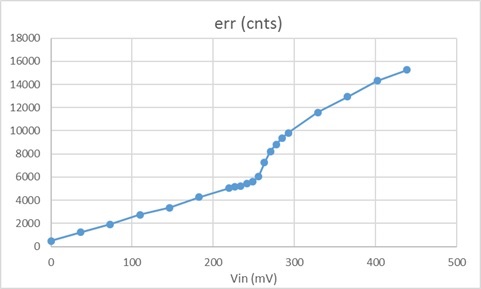
DDC118 Linearity Issue – as shown in the test data plot (Fig.1). The issue is that, the DDC118 linearity has a sudden change in the middle of the input signal.

The test was done with the test circuit as shown in Fig. 2. A constant current source, Ic (7.31uA), is applied to the resistor RT. Then the buffer op-amp output voltage is Ic*RT. The 10Mohm resistor converts the voltage into current input to one of the DDC118 inputs. With different RT resistor value, DDC118 counts were logged and converted to the measured resistance and compared with the true RT value to calculate out the measurement error -- the vertical axis of the plot. The DDC118 setting is: range 111, integration time 5 ms. At the setting, the linearity change occurred at ADC counts of around 400,000 (RT = 35kohm to 40 kohm).

AskTI-DDC118 Issue.pdf

  • Hi Steven,

    This is very strange. Looks very big. Here when we measure linearity we do have a similar setup with a large resistor, on the order of your 10MOhm. But we apply a voltage on that resistor with a precise DAC (lab DC source). Even more, we don't trust that voltage and we measure it with an even more precise voltmeter. Did you measure the voltage at the output of the amplifier on your figure to see if the break is there? Also I would think that changing RT is not very precise (resistor) but you may be doing this for some reason I don't know (like RT is your sensor or something...). So, my first suspect is the amplifier. Do you see this in other channels of the device or in other devices?

    Regards,
    Eduardo

  • Hello Eduardo,

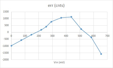
    Thanks for your quick response.  I repeated the test today. This time I measured the voltage at the output of the op-amp and monitored the actual ADC counts. I got the same error pattern. Please see attached. The horizontal axis is the measured voltage at the op-amp output – i.e., the input to the ADC through the 10Mohm resistor. The vertical axis is the error (= the logged ADC counts – calculated).  As you can see, the ADC data is pretty linear at the input voltage below 250mV (ADC input current of 25nA). After that it ramp up quickly and stay linear again at a different slope.

    The input voltage and the op-amp (unit gain) circuit is pretty precise and linear. We used a precise resistor box. The constant current Ic (7.31uA) was very stable. We tested and found the data is within 0.1 mV – this is the DMM resolution.

  • Hi Steven,

    Sorry my fault, just checked the vertical axis, didn't notice it was the error (measured-ideal). But still:

    1. Your setup looks ok. Once you are plotting DDC output vs voltage at the output of the opamp, we can basically forget about what you got before that output. 
    2. You know this but just to do some quick check... If you put 400mV across 10MOhms, you inject 40nA. In 5ms that's 200pC or 700k codes (give it or take). 
    3. The typical INL error is given (for Range 5) as ±0.01% Reading ± 0.5ppm FSR. Let's assume that it is more or less the same for Range 7. So, in 200pC one should expect about 0.01% x 200pC or 70 codes!
    4. That should be the typ error at the 400mV to a best fit line. Not sure how you computed the "ideal" line but it doesn't look like you completely removed the gain error from the best fit line as it keeps increasing. 
    5. Nevertheless, I feel that even if you do that and get a better line going through that graph, the error will be much bigger than 70 (or ~45 for the inflection point you are looking at). Your vertical scale is in the thousands...

    So, trying to think through this... Some questions:

    1. Maybe I missed it... where is the DDC? In your board or on our EVM?
    2. How many DDC118 have you checked?
    3. Does it happen in all the channels?
    4. Can you swith the 10MOhms for say 5MOhms (just solder another 10MOhms in parallel for easy job) and see where the kink happens respect to the output voltage of the amplifier?
    5. Have you checked your supplies (none clipping, current limited)? Do you see them change consumption at that point?
    6. How about your reference? Can you check the voltage at that pin?

    Thank you!
    Edu

  • Hi Edu,

    Here is brief answer to your questions:

    1. The DDC is on our board.
    2. We checked two boards. Same behavior.
    3. It happened on the four channels – AIN3, 4, 7 & 8. I checked on AIN1 yesterday and did not seem to be reproduceable on this input. I’ll double check on a different board.
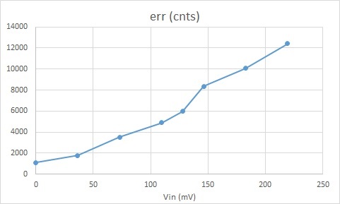
    4. Switched to 5Mohm. Seems reproduceable with slight difference. See the test data plot below.
    5. The +5VA was stable.
    6. The 4.096V VREF was accurate and stable.


    Thanks,

  • Edu,

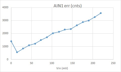
    I tested another board. The issue is not reproduceable on AIN1. Here is the data plot. The previous plot is data from AIN4. AIN1 and AIN4 have different timing.

  • BTW, the AIN1 uses longer integrating time.  This is why you see the Vin level is less than the previous plots.

  • Hi Steven,

    The 5MOhm test is actually pretty close, as you said. I mean, you can perceive the kink that before was at 250mV and 125mV now. Non-linearity levels are similar too.

    It is interesting that you see the same pattern in 3, 4, 7 and 8. They are all on the same side of the IC and they also use the 2nd cycle of the respective ADC to do the conversion in every cycle.

    The other side (ch1) looks more linear except for the first kink. Where you saturating for the first data point? It is difficult to say if a best fit line (without that kink) would get you to the spec numbers:

    1. How many points are you taking at every voltage level to compute that graph point?
    2. Can you share the raw data, under the same conditions for all the channels?
    3. Where are the input signals coming from?
    4. Are there any differences in the layout between one and the other sides? Are you shielding those lines? I am also looking for any other traces going near by those, including what are supposed to be DC traces like power and reference...
    5. Are you exciting all channels at the same time with the same signal or have only connection to the one you are looking and leaving the others floating?
    6. Do you have the whole setup in a shielded box?
    7. What exact part number are you using?
    8. Can you share CLK, CONV, DCLK freq. and pin 5 level?
    9. When are you starting to read the data after DVALID?

    Thank you!

    Edu

  • Here are brief answer to your questions:

    1. I read the display and record the value in the middle. Usually I observe the displayed value drifted about 200 to 500 counts.
    2. See at the end of this message for one set of data. As said, the data looks the same for all the channels. No abnormal.
    3.  The input signal came from the output of the op-amp. Monitored with DMM and very accurate and stable.
    4. We checked the layout. No issue found. The inputs are shielded with GND as recommended in the datasheet. No power rail or other signals nearby. I’ll double check.
    5. I tried both. No difference.
    6. Not in a shielded box. This may explain why noise about several hundred counts.
    7. DDC118IRTC
    8. CLK=4MHz, DCLK about 400kHz. Pin 5 shorted to GND (0V). Will send the CONV waveform later.
    9. About 8.3 us after the falling edge of DVALID. 

    Vin(mV)                ADC cnts              Cal(cnts)              err (cnts)

    0             4856      4096      760

    73.1       115111  113169  1942

    146.2     225624  222243  3381

    219.3     336205  331316  4889

    255.85   391750  385853  5897

    292.4     450173  440390  9783

    365.5     562368  549463  12905

    438.6     673752  658537  15215

  • Edu,

    Please see the signal waveform below.  Please notice the first falling edge pulse (500us) of CONV.  For some reason, the micro sent 4 clock pulses.  This is not intended.  Will this have something to do with the issue?

  • Hi Steven,

    I am having hard time reading the time scale. Is that 5ms/div? 

    Is it fair to say that you are changing on the fly integration times? Certainly I don't think you can expect the same code if you do that (obvious) so I am missing something...

    If you can plot DVALID is also good.

    In order to compute the proper DC code for a given input you can't combine A and B sides. Both have different offset and gain errors as they go through different integrators. You can to either add A+B and take them as single sample or correct A side and B side independently and then put the samples together.

    The kind of error we are looking for is super small. ~100 codes. So, you can't do that just by looking at the display. Need to store, say, 1000 samples of the A side and get its average. We can start by seeing if it gets linear within the A side alone (if you don't want to bother yet with offset and gain calibration).

    Also noise is super critical. Its average may not be zero during the period of time that you look at. So, certainly recommend a shielded box for any DDC related stuff. May not be the issue here though as problem seems repeatable and of larger scale.

    Let's clarify some of these and see...
    Edu

  • Hello Edu,

    Yes, the time scale is 5 ms / div.  The DVALID is not shown in the plot.  But it is a narrow pulse, as described in the datasheet, right before the DCLK pulse train -- 8.3 us earlier.  It follows the datasheet and I don't see issue.

    As for the noise of hundreds of counts, that is within our expectation.  Now our problems is that we have the linearity error of thousands of counts that we con't eliminate through calibration.  Please see the plot in the message of April 23.  Where you can see that, since the error associated with the Vin range below 250mV is linear, we can handle it through calibration.  But that does not apply to the Vin higher than 250mV.  The linearity changed with a big jump and we don't know why.

    How about you let me know your email and I can send you data or plot that way?

    Thanks,

    Steven

  • Hi Steven,

    I just PM you with my email. Please let me know if you didn't get it...

    We can exchange data there but just for the benefit of others that may be reading this with similar problems, let's continue the discussion here, if you don't mind...

    1. Can you let me know if you are changing the integration time from sample to sample? That's how it looks from the CONV timing...
    2. Assuming that CONV period is constant, are you separating A and B side sequences OR calibrating them to remove offset and gain differences between both sides?
    3. Looking at your timing diagram, looks weird:
      1. First I can see CONV high. Let's assume that some read happened there.
      2. Then during the next CONV (short one, low) you would get a DVALID and read the data. That would be the first DOUT train.
      3. I assume that CONV low is long enough (~500us) for continuous mode (please let me know if not the case). The weird thing is that then CONV goes high. That would trigger the ADC to do its work and output the data relatively soon but I don't see any read. Maybe DVALID came but your MCU didn't give any DCLK? Or maybe it comes before you actually finished reading the previous one? So they are overlapped? 
      4. The ones that you are circling look correct. I mean, The first one is the readout for the ADC conversion of the long (~13ms) CONV integration, and the 2nd one is for the shorter integration (CONV low for 5ms). 

    Noise wise, it is not so much a matter of being ok or not for you from a performance perspective, but more that those levels of noise can degrade also the accuracy (noise DC value may not be zero on an integration period). But anyhow I think we got bigger problems than that... Let's tackle the above first...

    Regards,
    Edu

  • Hi Edu,

    We only log the data in what I circled. As for previous two cycles including the short pulse, we got DVALID and s/w clock out two bits but does not record it. We tried not clocking the data and found it does not impact what are read out in the circled two cycles.

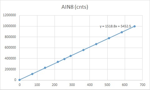
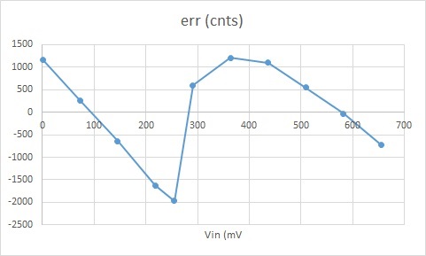
    I tried a different timing. This time there is no 500us short pulse. That is, we only have the 5ms negative pulse for B side integration. I got a different nonlinearity error pattern like the plot below:

    That is quite different than the test result with original timing. Here is the plot of the tested data at the same setup and condition except the timing difference .

    Seems the timing does impact the linearity. 1000 count is about 0.1% FSR. Just want to confirm if this is the design of the DDC118, and it should be consistent from unit to unit and no drift over ambient and time.

    Thanks,

    Steven

  • Hi Steven,

    So, just to make sure, you still have 2 integration times that are different, right? I mean, you have a long A and then the 5ms B, and then repeat, right? And you are taking A and B sides samples with one given DC input. Is that right? How do you correct for the two very different integration times? I mean, you say you capture on the circled instant. That is data for A and B. Maybe you are just using A samples or B samples on your calculation?

    It is kind of difficult to eyeball a best fit line on those graphs (although this time you did a better job) but honestly, the results still look off by a lot (maybe 2-3x). Unfortunately we don't have INL plots on the DDC118 but if you check the DDC264 datasheet, which actually by spec is 2.5x worse than the DDC118 (0.01% of reading on DDC118 vs 0.025% of reading on the DDC264) you can see some examples. Vertical scales are on the hundreds, not on the thousands. As such, I would not expect them to be consistent unit over unit or ambient conditions as I don't know where the error comes. Well, I guess consistent is a relative term ("within some margin") but still, I would like to understand that at least the data is being taken correctly before blessing these.

    Please send me by email 1000 raw samples for A and 1000 raw samples for B, i.e., 2000 consecutive samples as they come from the DDC, at every one of the input currents (voltages) you are taking. You can do that just for one of the channels but it would be nice if we get all 8. Excel file for instance works. (1000 is a ball park, if you can do 1024 or whatever number, 20k, etc... it works...). Also, please include the conditions (range and CONV times).

    Have a nice weekend!

    Edu

  • Hello Edu,

    Yes, we’ve a long integration time for A and short for B (5ms). We just use the B side samples for the calculation of B side signal counts.

    To test as we discussed, we changed the CONV timing to 5ms for both A and B side inputs. Now the nonlinearity was not reproduceable. That is another confirm that the long A side integration time causes the B side integrator to saturation that impacts the signal sensing linearity. Then our proposed solution will be to reduce the B side input signal level to avoid integrator saturation.  Please let me know if anything else.

    Thanks,

    Steven

  • Excellent, Steven! Thanks a lot for reporting back!

    Just to make sure, when you say "nonlinearity was not reproduceable" you meant that the problem is not there and now you get close to the datasheet value, right?

    Assuming this is correct, I will just recap for the other folks reading the thread... There were two different integration times alternating, for A and B sides of the same channel, one longer than the other. You only cared about one of the two (the shorter one) but the input signal was present during the two of them. As you increased the input signal, the previous sample (on the longer integration time) would start at one point saturating the input amplifier and affect the next sample, the one you cared about. Removing the saturation from the previous sample solved the problem.

    More in detail, as I am not sure we explained this anywhere before, as the integrated current in a given integrator starts to exceed the full-scale charge of the integrator, the amplifier saturates and the integrator is no more in close loop. Whatever current comes after that in the same integration period, it still flows in the capacitor but now, as the output of the amplifier is set (by the saturation), the input actually starts rising (no virtual ground anymore). If this current/charge is large enough, eventually the voltage will raise to the point the input ESD turns on, taking part of that current to ground and limiting the input voltage to a diode drop (~0.4-0.6V). Even if one does not care about this because one doesn't want that sample anyhow, the problem is that this same voltage is across some parasitic capacitance at the input (input trace, detector capacitance...). I.e., that parasitic capacitance holds some charge at the end of the integration period. When one switches from one integration to the other (from A to B or vice versa) there is no reset of the input, it is simply disconnected from one integrator and connected back to the other (I believe almost with a make before break). So, that charge fruit of the saturation on the previous period, stored on that capacitor, gets dumped now into the integration of interest and that distorts the final result.

    Well, I'll go ahead and close the thread. Please comment if there are any issues...

    Best regards,
    Edu

  • Hello Edu,

    That is right.  Thanks very much for your time, efforts and all the great technical details provided!

    Great Support!

    Steven

  • Great! This was a tricky one. Thank you Steven for reporting back for the benefit of others.

    Have a nice day!