Other Parts Discussed in Thread: ADS7951, ADS7891
Hello,
I'm coping with a problem concerning A/D measurements done with the AD-converter ADS7951.
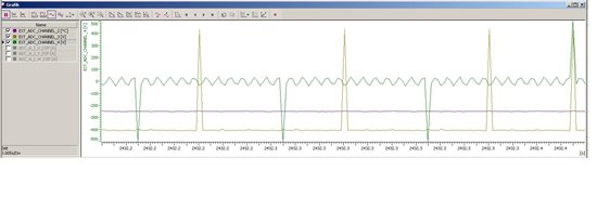
At first I'll describe the application it is used in: this is an high power inverter (~15kW) where the ADC converts the measured voltage values of the IGBT-temperature NTC, the divided down input voltage (up to 400V) and the divided down phase to phase voltage. In low power mode the reported measurement values are correct. At 400V input voltage and full output load the converted values are faulty. There are positive or negative distortions on either one or multiple channels. The idea was that the measurements were done in a switching moment. So the approach to solving the problem was to shift the measurement into a gap where there is no switching of the IGBTs (falling edge of chip select is at the start of the gap). But this did not help.
So one first question is if somebody had a similar problem before.
Up to now, the opinion was that the channel to convert is chosen at a falling edge of the chip select (CS) signal. But in the data sheet on page 23 it is described in a different way. There it says: "the acquisition phase starts on the 14th SCLK rising edge. On the next CS falling edge the acquisition phase will end, and the device starts a new frame." So this would mean that there is a very long acquisition time. This could explain why the solution described above did not work. Is the acquisition phase (channel connected to the internal capacitor, compare figure 59 on data sheet) really this long?
Is the defined over voltage recovery time of 150ns (specified in electrical characteristics on page 7) valid for all voltages (there is no condition specified)?
I'm looking forward to answers!
Thanks and best regards,
T. Abele