This thread has been locked.

If you have a related question, please click the "Ask a related question" button in the top right corner. The newly created question will be automatically linked to this question.

DAC38RF80EVM: Achieving desired sampling rate and conflicts between GUI and datasheet

Part Number: DAC38RF80EVM
Other Parts Discussed in Thread: LMK04828, ADC32RF44

Hello,

I am currently trying to bring up the eval board for the DAC38RF30. I am operating with an LMF of 821.

I am trying to avoid injecting a clock onto the board and just use the 122.88MHz oscillator that is connected to the OSCin port on the LMK04828. By using VCO0 on the LMK I am able to generate a VCO frequency of 2457.6MHz and divide it down to 1228.8MHz (2457.6/2) for the single ended DAC clock and 153.6MHz (2457.6/16) for my FPGA. I am doing it this way so I will need to generate 8 sample of I data and 8 samples of Q data every clock cycle on my FPGA. The datasheet for this part specifies various LMFSHd values for the JESD interface but it only gives example of 1 or 2 I and Q sample per channel per frame, but I assume I am able to give it more, in this case 8. Please let me know if this is incorrect.

My first question is this: With the 6x interpolation on, does that bring my theoretical sampling frequency up 6 times or down? Does my new sampling frequency become 7372.8‬MHz (1228.8 * 6) or do I need to supply my DAC with a 7372.8MHz clock so that when it interpolates it is only sampling the data from the FPGA at 1228.8MHz?

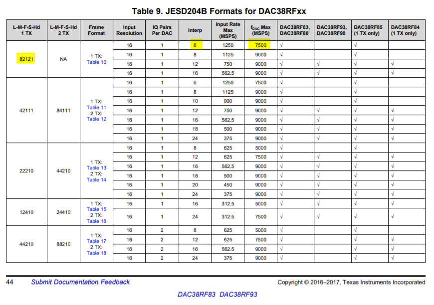
My second question is about a discrepancy between the datasheet for this DAC and the GUI to operate its EVM. The following is from the DAC38RFxx data sheet (I highlighted the areas of interest):
And the following is from the DAC38RF3x EVM GUI:
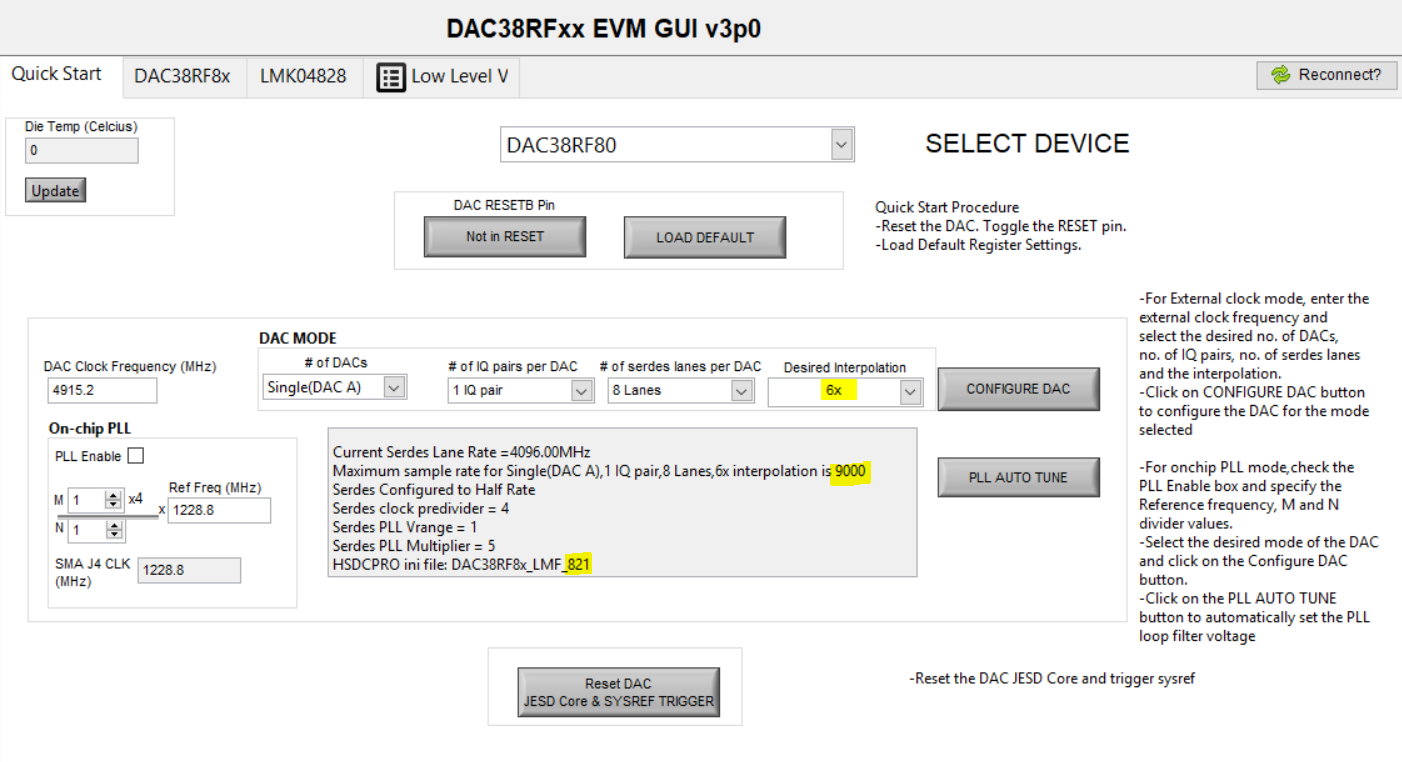
As you can see, the datasheet specifies a maximum sample rate that is different than the maximum specified by the GUI. Which one is accurate?

Thank you for your time.

  • Jacob,

    In the 82121 mode, you can only get 2 samples per frame. The part can only do 1 or 2 samples per frame. This is the -S- parameter and cannot be changed.

    "My first question is this: With the 6x interpolation on, does that bring my theoretical sampling frequency up 6 times or down? Does my new sampling frequency become 7372.8‬MHz (1228.8 * 6) or do I need to supply my DAC with a 7372.8MHz clock so that when it interpolates it is only sampling the data from the FPGA at 1228.8MHz?"  

    The DAC sample rate divided by the interpolation factor = DAC data rate from the FPGA. If you are using 6x interpolation, the FPGA would need to send data at 1228.8Msps and the DAC clock would have to be at 7372.8Msps. 

    The GUI is correct and the data sheet is wrong for your last question.

    Regards,

    Jim

  • Jim,

    Thank you for answering my data rate and GUI/datasheet questions. That is very helpful.

    Regarding the LMFS parameters, if the data rate coming from the FPGA is 1228.8Msps and I am producing 2 samples per clock cycle (2 I samples and 2 Q samples) then I would need to clock my FPGA at 614.4MHz, which seems way too fast. I thought the flexibility of the JESD interface was in the speed at which I could run my FPGA (ex: if I wanted my FPGA clock to be 4 times less than my DAC clock then I just need to provide 4 samples every FPGA clock cycle, same for 2 and 8).

    Is this not the case? Do I either need to run my FPGA at extremely high clocking rates or greatly reduce the sampling rate of my DAC? Both cases sound less than ideal. It could be that the IP core I am using to send the data packages it up in a certain way to avoid these outcomes (I am using the JESD204 v7.2 Xilinx IP core for context).

    I will mention that I was able to get the ADC32RF44 without decimation to produce 8 sample for both ADCs (16 total) on each FPGA clock cycle. The LMFS values on the datasheet for that device don't include this configuration either.

    Thank you,

    Jake

  • Jake,

    The FPGA vendor you are using for your board should have documentation explaining how to use a lower clock rate for the FPGA. This is usually done by packing samples in a 32 or 64 bit words. Attached is a document showing the architecture used by the TI TSW14J56EVM (Intel FPGA TI capture/pattern generator card). 

    Regards,

    Jim


    5824.TSW14J56 RevD MC firmware design document.doc