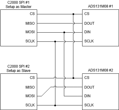
Hi expert,
I am completing a Design using one C2000 two SPI module connecting two ADS131. two ADS131 are clocking by one external 8M crystal.
I test every single ADS131 can work normally. And I want to enable it in the same code.
So I edit the hal.c / hal.h / ads131m0x.c , but I found it can not work together, which means I can not see the SCLK between C2000 and ADS131.
When I change the sequence of these code in main.c, I can see ADS131-1 SCLK and ADS131-2 SCLK, but not at same time.
    writeSingleRegister(0x02, 0x0010);
//    writeSingleRegister2(0x02, 0x0010);
    writeSingleRegister(0x03, 0xFF43);// external reference ENABLED, OSR 128 32k SAMPLE RATE
//    writeSingleRegister2(0x03, 0xFF43);
    SysCtl_delay(10000);

    initSPI2(SPIA_BASE);
    SPI_clearInterruptStatus(SPIA_BASE, SPI_INT_RXFF );
    SPI_resetRxFIFO(SPIA_BASE);
    SPI_resetTxFIFO(SPIA_BASE);
    Interrupt_enable(INT_SPIA_RX);

    //
    // Enable Global Interrupt (INTM) and realtime interrupt (DBGM)

    SPI_resetRxFIFO(SPIA_BASE);
    //
    EINT;
    ERTM;

    readDataTx(SPIA_BASE);

//todo add SPIB INIT
    ///////////////SPIB INIT/////////////////////////
// TODO Change to initSPI2
	writeSingleRegister2(0x02, 0x0010);
	writeSingleRegister2(0x03, 0xFF43);
	SysCtl_delay(10000);

    initSPI2(SPIB_BASE);
    //    SPI_enableInterrupt(SPIA_BASE, SPI_INT_RXFF|SPI_INT_TXFF);
    SPI_clearInterruptStatus(SPIB_BASE, SPI_INT_RXFF );
    SPI_resetRxFIFO(SPIB_BASE);
    SPI_resetTxFIFO(SPIB_BASE);
    Interrupt_enable(INT_SPIB_RX);
    //Interrupt_enable(INT_SPIA_TX);

    // Enable Global Interrupt (INTM) and realtime interrupt (DBGM)

    SPI_resetRxFIFO(SPIB_BASE);
    //
    EINT;
    ERTM;

    readDataTx(SPIB_BASE);
I almost copied the driver code for every function I used. But not for these
static uint16_t             registerMap[NUM_REGISTERS];

void restoreRegisterDefaults(void)
Because I suppose it should be the same for each ADS131, but I can tell which one by call different SPI module to write.
Could you kindly tell me where I did wrong?
Attached relevant code, xTIDA010086.h is writen by our team.
/**
 * \copyright Copyright (C) 2019 Texas Instruments Incorporated - http://www.ti.com/
 *
 *  Redistribution and use in source and binary forms, with or without
 *  modification, are permitted provided that the following conditions
 *  are met:
 *
 *    Redistributions of source code must retain the above copyright
 *    notice, this list of conditions and the following disclaimer.
 *
 *    Redistributions in binary form must reproduce the above copyright
 *    notice, this list of conditions and the following disclaimer in the
 *    documentation and/or other materials provided with the
 *    distribution.
 *
 *    Neither the name of Texas Instruments Incorporated nor the names of
 *    its contributors may be used to endorse or promote products derived
 *    from this software without specific prior written permission.
 *
 *  THIS SOFTWARE IS PROVIDED BY THE COPYRIGHT HOLDERS AND CONTRIBUTORS
 *  "AS IS" AND ANY EXPRESS OR IMPLIED WARRANTIES, INCLUDING, BUT NOT
 *  LIMITED TO, THE IMPLIED WARRANTIES OF MERCHANTABILITY AND FITNESS FOR
 *  A PARTICULAR PURPOSE ARE DISCLAIMED. IN NO EVENT SHALL THE COPYRIGHT
 *  OWNER OR CONTRIBUTORS BE LIABLE FOR ANY DIRECT, INDIRECT, INCIDENTAL,
 *  SPECIAL, EXEMPLARY, OR CONSEQUENTIAL DAMAGES (INCLUDING, BUT NOT
 *  LIMITED TO, PROCUREMENT OF SUBSTITUTE GOODS OR SERVICES; LOSS OF USE,
 *  DATA, OR PROFITS; OR BUSINESS INTERRUPTION) HOWEVER CAUSED AND ON ANY
 *  THEORY OF LIABILITY, WHETHER IN CONTRACT, STRICT LIABILITY, OR TORT
 *  (INCLUDING NEGLIGENCE OR OTHERWISE) ARISING IN ANY WAY OUT OF THE USE
 *  OF THIS SOFTWARE, EVEN IF ADVISED OF THE POSSIBILITY OF SUCH DAMAGE.
 *
 */

#include "ads131m0x.h"


//****************************************************************************
//
// Internal variables
//
//****************************************************************************

// Array used to recall device register map configurations */
static uint16_t             registerMap[NUM_REGISTERS];

// Array of SPI word lengths
const static unsigned char        wlength_byte_values[] = {2, 3, 4, 4};


//****************************************************************************
//
// Internal function prototypes
//
//****************************************************************************

unsigned char     buildSPIarray(const uint16_t opcodeArray[], unsigned char numberOpcodes, unsigned char byteArray[]);
uint16_t    enforce_selected_device_modes(uint16_t data);
unsigned char     getWordByteLength(void);


//*****************************************************************************
//
//! Getter function to access registerMap array from outside of this module.
//!
//! \fn uint16_t getRegisterValue(unsigned char address)
//!
//! NOTE: The internal registerMap arrays stores the last know register value,
//! since the last read or write operation to that register. This function
//! does not communicate with the device to retrieve the current register value.
//! For the most up-to-date register data or retrieving the value of a hardware
//! controlled register, it is recommend to use readSingleRegister() to read the
//! current register value.
//!
//! \return unsigned 16-bit register value.
//
//*****************************************************************************
uint16_t getRegisterValue(unsigned char address)
{
    assert(address < NUM_REGISTERS);
    return registerMap[address];
}


//*****************************************************************************
//
//! Example start up sequence for the ADS131M0x.
//!
//! \fn void adcStartup(void)
//!
//! Before calling this function, the device must be powered,
//! the SPI/GPIO pins of the MCU must have already been configured,
//! and (if applicable) the external clock source should be provided to CLKIN.
//!
//! \return None.
//
//*****************************************************************************
void adcStartup(void)
{
	/* (OPTIONAL) Provide additional delay time for power supply settling */
	delay_ms(50);

	/* (REQUIRED) Set nRESET pin high for ADC operation */
	setSYNC_RESET(HIGH);

	/* (OPTIONAL) Toggle nRESET pin to ensure default register settings. */
	/* NOTE: This also ensures that the device registers are unlocked.	 */
	toggleRESET();

    /* (REQUIRED) Initialize internal 'registerMap' array with device default settings */
	restoreRegisterDefaults();

    /* (OPTIONAL) Validate first response word when beginning SPI communication: (0xFF20 | CHANCNT) */
	uint16_t response = sendCommand(OPCODE_NULL);
	uint16_t response2 = sendCommand2(OPCODE_NULL);

	/* (OPTIONAL) Define your initial register settings here */
    writeSingleRegister(CLOCK_ADDRESS, (CLOCK_DEFAULT & ~CLOCK_OSR_MASK) | CLOCK_OSR_256);
	writeSingleRegister2(CLOCK_ADDRESS, (CLOCK_DEFAULT & ~CLOCK_OSR_MASK) | CLOCK_OSR_256);

    /* (REQUIRED) Configure MODE register settings
     * NOTE: This function call is required here for this particular code implementation to work.
     * This function will enforce the MODE register settings as selected in the 'ads131m0x.h' header file.
     */
    writeSingleRegister(MODE_ADDRESS, MODE_DEFAULT);
	writeSingleRegister2(MODE_ADDRESS, MODE_DEFAULT);

    /* (OPTIONAL) Read back all registers */

	/* (OPTIONAL) Check STATUS register for faults */
}


//*****************************************************************************
//
//! Reads the contents of a single register at the specified address.
//!
//! \fn uint16_t readSingleRegister(unsigned char address)
//!
//! \param address is the 8-bit address of the register to read.
//!
//! \return Returns the 8-bit register read result.
//
//*****************************************************************************
uint16_t readSingleRegister(unsigned char address)
{
	/* Check that the register address is in range */
	assert(address < NUM_REGISTERS);

// Build TX and RX byte array
#ifdef ENABLE_CRC_IN
    unsigned char dataTx[8] = { 0 };      // 2 words, up to 4 bytes each = 8 bytes maximum
    unsigned char dataRx[8] = { 0 };
#else
    unsigned char dataTx[4] = { 0 };      // 1 word, up to 4 bytes long = 4 bytes maximum
    unsigned char dataRx[4] = { 0 };
#endif
    uint16_t opcode = OPCODE_RREG | (((uint16_t) address) << 7);
    unsigned char numberOfBytes = buildSPIarray(&opcode, 1, dataTx);

	// [FRAME 1] Send RREG command
	spiSendReceiveArrays(dataTx, dataRx, numberOfBytes);

	// [FRAME 2] Send NULL command to retrieve the register data
	registerMap[address] = sendCommand(OPCODE_NULL);

	return registerMap[address];
}

uint16_t readSingleRegister2(unsigned char address)
{
	/* Check that the register address is in range */
	assert(address < NUM_REGISTERS);

// Build TX and RX byte array
#ifdef ENABLE_CRC_IN
    unsigned char dataTx[8] = { 0 };      // 2 words, up to 4 bytes each = 8 bytes maximum
    unsigned char dataRx[8] = { 0 };
#else
    unsigned char dataTx[4] = { 0 };      // 1 word, up to 4 bytes long = 4 bytes maximum
    unsigned char dataRx[4] = { 0 };
#endif
    uint16_t opcode = OPCODE_RREG | (((uint16_t) address) << 7);
    unsigned char numberOfBytes = buildSPIarray(&opcode, 1, dataTx);

	// [FRAME 1] Send RREG command
	spiBSendReceiveArrays(dataTx, dataRx, numberOfBytes);

	// [FRAME 2] Send NULL command to retrieve the register data
	registerMap[address] = sendCommand2(OPCODE_NULL);

	return registerMap[address];
}


//*****************************************************************************
//
//! Writes data to a single register.
//!
//! \fn void writeSingleRegister(unsigned char address, uint16_t data)
//!
//! \param address is the address of the register to write to.
//! \param data is the value to write.
//!
//! This command will be ignored if device registers are locked.
//!
//! \return None.
//
//*****************************************************************************
void writeSingleRegister(unsigned char address, uint16_t data)
{
    /* Check that the register address is in range */
    assert(address < NUM_REGISTERS);

    // (OPTIONAL) Enforce certain register field values when
    // writing to the MODE register to fix the operation mode
    if (MODE_ADDRESS == address)
    {
        data = enforce_selected_device_modes(data);
    }

    // Build TX and RX byte array
#ifdef ENABLE_CRC_IN
    unsigned char dataTx[12] = { 0 };     // 3 words, up to 4 bytes each = 12 bytes maximum
    unsigned char dataRx[12] = { 0 };
#else
    unsigned char dataTx[8] = { 0 };      // 2 words, up to 4 bytes long = 8 bytes maximum
    unsigned char dataRx[8] = { 0 };
#endif
    uint16_t opcodes[2];
    opcodes[0] = OPCODE_WREG | (((uint16_t) address) << 7);
    opcodes[1] = data;
    unsigned char numberOfBytes = buildSPIarray(&opcodes[0], 2, dataTx);

    // Send command
    spiSendReceiveArrays(dataTx, dataRx, numberOfBytes);

    // Update internal array
    registerMap[address] = data;

    // (RECOMMENDED) Read back register to confirm register write was successful
    readSingleRegister(address);

    // NOTE: Enabling the CRC words in the SPI command will NOT prevent an invalid W
}

void writeSingleRegister2(unsigned char address, uint16_t data)
{
    /* Check that the register address is in range */
    assert(address < NUM_REGISTERS);

    // (OPTIONAL) Enforce certain register field values when
    // writing to the MODE register to fix the operation mode
    if (MODE_ADDRESS == address)
    {
        data = enforce_selected_device_modes(data);
    }

    // Build TX and RX byte array
#ifdef ENABLE_CRC_IN
    unsigned char dataTx[12] = { 0 };     // 3 words, up to 4 bytes each = 12 bytes maximum
    unsigned char dataRx[12] = { 0 };
#else
    unsigned char dataTx[8] = { 0 };      // 2 words, up to 4 bytes long = 8 bytes maximum
    unsigned char dataRx[8] = { 0 };
#endif
    uint16_t opcodes[2];
    opcodes[0] = OPCODE_WREG | (((uint16_t) address) << 7);
    opcodes[1] = data;
    unsigned char numberOfBytes = buildSPIarray(&opcodes[0], 2, dataTx);

    // Send command
    spiBSendReceiveArrays(dataTx, dataRx, numberOfBytes);

    // Update internal array
    registerMap[address] = data;

    // (RECOMMENDED) Read back register to confirm register write was successful
    readSingleRegister2(address);

    // NOTE: Enabling the CRC words in the SPI command will NOT prevent an invalid W
}


//*****************************************************************************
//
//! Reads ADC data.
//!
//! \fn bool readData(adc_channel_data *DataStruct)
//!
//! \param *DataStruct points to an adc_channel_data type-defined structure/
//!
//! NOTE: Should be called after /DRDY goes low, and not during a /DRDY falling edge!
//!
//! \return Returns true if the CRC-OUT of the data read detects an error.
//
//*****************************************************************************
bool readData(adc_channel_data *DataStruct)
{
    int i;
    unsigned char crcTx[4]                        = { 0 };
    unsigned char dataRx[4]                       = { 0 };
    unsigned char bytesPerWord                    = getWordByteLength();

#ifdef ENABLE_CRC_IN
    // Build CRC word (only if "RX_CRC_EN" register bit is enabled)
    uint16_t crcWordIn = calculateCRC(&DataTx[0], bytesPerWord * 2, 0xFFFF);
    crcTx[0] = upperByte(crcWordIn);
    crcTx[1] = lowerByte(crcWordIn);
#endif

    /* Set the nCS pin LOW */
    setCS(LOW);

    // Send NULL word, receive response word
    for (i = 0; i < bytesPerWord; i++)
    {
        dataRx[i] = spiSendReceiveByte(0x00);
    }
    DataStruct->response = combineBytes(dataRx[0], dataRx[1]);

    // (OPTIONAL) Do something with the response (STATUS) word.
    // ...Here we only use the response for calculating the CRC-OUT
    //uint16_t crcWord = calculateCRC(&dataRx[0], bytesPerWord, 0xFFFF);

    // (OPTIONAL) Ignore CRC error checking
    uint16_t crcWord = 0;

    // Send 2nd word, receive channel 1 data
    for (i = 0; i < bytesPerWord; i++)
    {
        dataRx[i] = spiSendReceiveByte(crcTx[i]);
    }
    DataStruct->channel0 = signExtend(&dataRx[0]);
    //crcWord = calculateCRC(&dataRx[0], bytesPerWord, crcWord);

#if (CHANNEL_COUNT > 1)

    // Send 3rd word, receive channel 2 data
    for (i = 0; i < bytesPerWord; i++)
    {
        dataRx[i] = spiSendReceiveByte(0x00);
    }
    DataStruct->channel1 = signExtend(&dataRx[0]);
    //crcWord = calculateCRC(&dataRx[0], bytesPerWord, crcWord);

#endif
#if (CHANNEL_COUNT > 2)

    // Send 4th word, receive channel 3 data
    for (i = 0; i < bytesPerWord; i++)
    {
        dataRx[i] = spiSendReceiveByte(0x00);
    }
    DataStruct->channel2 = signExtend(&dataRx[0]);
    //crcWord = calculateCRC(&dataRx[0], bytesPerWord, crcWord);

#endif
#if (CHANNEL_COUNT > 3)

    // Send 5th word, receive channel 4 data
    for (i = 0; i < bytesPerWord; i++)
    {
        dataRx[i] = spiSendReceiveByte(0x00);
    }
    DataStruct->channel3 = signExtend(&dataRx[0]);
    //crcWord = calculateCRC(&dataRx[0], bytesPerWord, crcWord);

#endif
#if (CHANNEL_COUNT > 4)

    // Send 6th word, receive channel 5 data
    for (i = 0; i < bytesPerWord; i++)
    {
        dataRx[i] = spiSendReceiveByte(0x00);
    }
    DataStruct->channel4 = signExtend(&dataRx[0]);
    //crcWord = calculateCRC(&dataRx[0], bytesPerWord, crcWord);

#endif
#if (CHANNEL_COUNT > 5)

    // Send 7th word, receive channel 6 data
    for (i = 0; i < bytesPerWord; i++)
    {
        dataRx[i] = spiSendReceiveByte(0x00);
    }
    DataStruct->channel5 = signExtend(&dataRx[0]);
    //crcWord = calculateCRC(&dataRx[0], bytesPerWord, crcWord);

#endif
#if (CHANNEL_COUNT > 6)

    // Send 8th word, receive channel 7 data
    for (i = 0; i < bytesPerWord; i++)
    {
        dataRx[i] = spiSendReceiveByte(0x00);
    }
    DataStruct->channel6 = signExtend(&dataRx[0]);
    //crcWord = calculateCRC(&dataRx[0], bytesPerWord, crcWord);

#endif
#if (CHANNEL_COUNT > 7)

    // Send 9th word, receive channel 8 data
    for (i = 0; i < bytesPerWord; i++)
    {
        dataRx[i] = spiSendReceiveByte(0x00);
    }
    DataStruct->channel7 = signExtend(&dataRx[0]);
    //crcWord = calculateCRC(&dataRx[0], bytesPerWord, crcWord);

#endif

    // Send the next word, receive CRC data
    for (i = 0; i < bytesPerWord; i++)
    {
        dataRx[i] = spiSendReceiveByte(0x00);
    }
    DataStruct->crc = combineBytes(dataRx[0], dataRx[1]);

    /* NOTE: If we continue calculating the CRC with a matching CRC, the result should be zero.
     * Any non-zero result will indicate a mismatch.
     */
    //crcWord = calculateCRC(&dataRx[0], bytesPerWord, crcWord);

    /* Set the nCS pin HIGH */
    setCS(HIGH);

    // Returns true when a CRC error occurs
    return ((bool) crcWord);
}

bool readData2(adc_channel_data *DataStruct)
{
    int i;
    unsigned char crcTx[4]                        = { 0 };
    unsigned char dataRx[4]                       = { 0 };
    unsigned char bytesPerWord                    = getWordByteLength();

#ifdef ENABLE_CRC_IN
    // Build CRC word (only if "RX_CRC_EN" register bit is enabled)
    uint16_t crcWordIn = calculateCRC(&DataTx[0], bytesPerWord * 2, 0xFFFF);
    crcTx[0] = upperByte(crcWordIn);
    crcTx[1] = lowerByte(crcWordIn);
#endif

    /* Set the nCS pin LOW */
    setCSB(LOW);

    // Send NULL word, receive response word
    for (i = 0; i < bytesPerWord; i++)
    {
        dataRx[i] = spiBSendReceiveByte(0x00);
    }
    DataStruct->response = combineBytes(dataRx[0], dataRx[1]);

    // (OPTIONAL) Do something with the response (STATUS) word.
    // ...Here we only use the response for calculating the CRC-OUT
    //uint16_t crcWord = calculateCRC(&dataRx[0], bytesPerWord, 0xFFFF);

    // (OPTIONAL) Ignore CRC error checking
    uint16_t crcWord = 0;

    // Send 2nd word, receive channel 1 data
    for (i = 0; i < bytesPerWord; i++)
    {
        dataRx[i] = spiBSendReceiveByte(crcTx[i]);
    }
    DataStruct->channel0 = signExtend(&dataRx[0]);
    //crcWord = calculateCRC(&dataRx[0], bytesPerWord, crcWord);

#if (CHANNEL_COUNT > 1)

    // Send 3rd word, receive channel 2 data
    for (i = 0; i < bytesPerWord; i++)
    {
        dataRx[i] = spiBSendReceiveByte(0x00);
    }
    DataStruct->channel1 = signExtend(&dataRx[0]);
    //crcWord = calculateCRC(&dataRx[0], bytesPerWord, crcWord);

#endif
#if (CHANNEL_COUNT > 2)

    // Send 4th word, receive channel 3 data
    for (i = 0; i < bytesPerWord; i++)
    {
        dataRx[i] = spiBSendReceiveByte(0x00);
    }
    DataStruct->channel2 = signExtend(&dataRx[0]);
    //crcWord = calculateCRC(&dataRx[0], bytesPerWord, crcWord);

#endif
#if (CHANNEL_COUNT > 3)

    // Send 5th word, receive channel 4 data
    for (i = 0; i < bytesPerWord; i++)
    {
        dataRx[i] = spiBSendReceiveByte(0x00);
    }
    DataStruct->channel3 = signExtend(&dataRx[0]);
    //crcWord = calculateCRC(&dataRx[0], bytesPerWord, crcWord);

#endif
#if (CHANNEL_COUNT > 4)

    // Send 6th word, receive channel 5 data
    for (i = 0; i < bytesPerWord; i++)
    {
        dataRx[i] = spiBSendReceiveByte(0x00);
    }
    DataStruct->channel4 = signExtend(&dataRx[0]);
    //crcWord = calculateCRC(&dataRx[0], bytesPerWord, crcWord);

#endif
#if (CHANNEL_COUNT > 5)

    // Send 7th word, receive channel 6 data
    for (i = 0; i < bytesPerWord; i++)
    {
        dataRx[i] = spiBSendReceiveByte(0x00);
    }
    DataStruct->channel5 = signExtend(&dataRx[0]);
    //crcWord = calculateCRC(&dataRx[0], bytesPerWord, crcWord);

#endif
#if (CHANNEL_COUNT > 6)

    // Send 8th word, receive channel 7 data
    for (i = 0; i < bytesPerWord; i++)
    {
        dataRx[i] = spiBSendReceiveByte(0x00);
    }
    DataStruct->channel6 = signExtend(&dataRx[0]);
    //crcWord = calculateCRC(&dataRx[0], bytesPerWord, crcWord);

#endif
#if (CHANNEL_COUNT > 7)

    // Send 9th word, receive channel 8 data
    for (i = 0; i < bytesPerWord; i++)
    {
        dataRx[i] = spiBSendReceiveByte(0x00);
    }
    DataStruct->channel7 = signExtend(&dataRx[0]);
    //crcWord = calculateCRC(&dataRx[0], bytesPerWord, crcWord);

#endif

    // Send the next word, receive CRC data
    for (i = 0; i < bytesPerWord; i++)
    {
        dataRx[i] = spiBSendReceiveByte(0x00);
    }
    DataStruct->crc = combineBytes(dataRx[0], dataRx[1]);

    /* NOTE: If we continue calculating the CRC with a matching CRC, the result should be zero.
     * Any non-zero result will indicate a mismatch.
     */
    //crcWord = calculateCRC(&dataRx[0], bytesPerWord, crcWord);

    /* Set the nCS pin HIGH */
    setCSB(HIGH);

    // Returns true when a CRC error occurs
    return ((bool) crcWord);
}

//*****************************************************************************
//
//! Sends the specified SPI command to the ADC (NULL, STANDBY, or WAKEUP).
//!
//! \fn uint16_t sendCommand(uint16_t opcode)
//!
//! \param opcode SPI command byte.
//!
//! NOTE: Other commands have their own dedicated functions to support
//! additional functionality.
//!
//! \return ADC response byte (typically the STATUS byte).
//
//*****************************************************************************
uint16_t sendCommand(uint16_t opcode)
{
    /* Assert if this function is used to send any of the following opcodes */
    assert(OPCODE_RREG != opcode);      /* Use "readSingleRegister()"   */
    assert(OPCODE_WREG != opcode);      /* Use "writeSingleRegister()"  */
    assert(OPCODE_LOCK != opcode);      /* Use "lockRegisters()"        */
    assert(OPCODE_UNLOCK != opcode);    /* Use "unlockRegisters()"      */
    assert(OPCODE_RESET != opcode);     /* Use "resetDevice()"          */

    // Build TX and RX byte array
#ifdef ENABLE_CRC_IN
    unsigned char dataTx[8] = { 0 };      // 2 words, up to 4 bytes each = 8 bytes maximum
    unsigned char dataRx[8] = { 0 };
#else
    unsigned char dataTx[4] = { 0 };      // 1 word, up to 4 bytes long = 4 bytes maximum
    unsigned char dataRx[4] = { 0 };
#endif
    unsigned char numberOfBytes = buildSPIarray(&opcode, 1, dataTx);

    /* Set the nCS pin LOW */
    setCS(LOW);

    // Send the opcode (and crc word, if enabled)
    int i;
    for (i = 0; i < numberOfBytes; i++)
    {
       dataRx[i] = spiSendReceiveByte(dataTx[i]);
    }

    /* Set the nCS pin HIGH */
    setCS(HIGH);

    // Combine response bytes and return as a 16-bit word
    uint16_t adcResponse = combineBytes(dataRx[0], dataRx[1]);
    return adcResponse;
}

uint16_t sendCommand2(uint16_t opcode)
{
    /* Assert if this function is used to send any of the following opcodes */
    assert(OPCODE_RREG != opcode);      /* Use "readSingleRegister()"   */
    assert(OPCODE_WREG != opcode);      /* Use "writeSingleRegister()"  */
    assert(OPCODE_LOCK != opcode);      /* Use "lockRegisters()"        */
    assert(OPCODE_UNLOCK != opcode);    /* Use "unlockRegisters()"      */
    assert(OPCODE_RESET != opcode);     /* Use "resetDevice()"          */

    // Build TX and RX byte array
#ifdef ENABLE_CRC_IN
    unsigned char dataTx[8] = { 0 };      // 2 words, up to 4 bytes each = 8 bytes maximum
    unsigned char dataRx[8] = { 0 };
#else
    unsigned char dataTx[4] = { 0 };      // 1 word, up to 4 bytes long = 4 bytes maximum
    unsigned char dataRx[4] = { 0 };
#endif
    unsigned char numberOfBytes = buildSPIarray(&opcode, 1, dataTx);

    /* Set the nCS pin LOW */
    setCSB(LOW);

    // Send the opcode (and crc word, if enabled)
    int i;
    for (i = 0; i < numberOfBytes; i++)
    {
       dataRx[i] = spiBSendReceiveByte(dataTx[i]);
    }

    /* Set the nCS pin HIGH */
    setCSB(HIGH);

    // Combine response bytes and return as a 16-bit word
    uint16_t adcResponse = combineBytes(dataRx[0], dataRx[1]);
    return adcResponse;
}


//*****************************************************************************
//
//! Resets the device.
//!
//! \fn void resetDevice(void)
//!
//! NOTE: This function does not capture DOUT data, but it could be modified
//! to do so.
//!
//! \return None.
//
//*****************************************************************************
void resetDevice(void)
{
    // Build TX and RX byte array
#ifdef ENABLE_CRC_IN
    unsigned char dataTx[8] = { 0 };      // 2 words, up to 4 bytes each = 8 bytes maximum
    //unsigned char dataRx[8] = { 0 };    // Only needed if capturing data
#else
    unsigned char dataTx[4] = { 0 };      // 1 word, up to 4 bytes long = 4 bytes maximum
    //unsigned char dataRx[4] = { 0 };    // Only needed if capturing data
#endif
    uint16_t opcode         = OPCODE_RESET;
    unsigned char numberOfBytes   = buildSPIarray(&opcode, 1, dataTx);

    unsigned char bytesPerWord    = wlength_byte_values[WLENGTH];
    unsigned char wordsInFrame    = CHANNEL_COUNT + 2;

    // Set the nCS pin LOW
    setCS(LOW);

    // Send the opcode (and CRC word, if enabled)
    int i;
    for (i = 0; i < numberOfBytes; i++)
    {
         spiSendReceiveByte(dataTx[i]);
    }

    // Finish sending remaining bytes
    for (i = numberOfBytes; i < (wordsInFrame * bytesPerWord); i++)
    {
        spiSendReceiveByte(0x00);
    }

    // NOTE: The ADS131M0x's next response word should be (0xFF20 | CHANCNT),
    // if the response is 0x0011 (acknowledge of RESET command), then the device
    // did not receive a full SPI frame and the reset did not occur!

    // Set the nCS pin HIGH
    setCS(HIGH);

    // tSRLRST delay, ~1ms with 2.048 MHz fCLK
    delay_ms(1);

    // Update register setting array to keep software in sync with device
    restoreRegisterDefaults();

    // Write to MODE register to enforce mode settings
    writeSingleRegister(MODE_ADDRESS, MODE_DEFAULT);
}


//*****************************************************************************
//
//! Sends the LOCK command and verifies that registers are locked.
//!
//! \fn bool lockRegisters(void)
//!
//! \return boolean to indicate if an error occurred (0 = no error; 1 = error)
//
//*****************************************************************************
bool lockRegisters(void)
{
    bool b_lock_error;

    // Build TX and RX byte array
#ifdef ENABLE_CRC_IN
    unsigned char dataTx[8] = { 0 };      // 2 words, up to 4 bytes each = 8 bytes maximum
    unsigned char dataRx[8] = { 0 };
#else
    unsigned char dataTx[4] = { 0 };      // 1 word, up to 4 bytes long = 4 bytes maximum
    unsigned char dataRx[4] = { 0 };
#endif
    uint16_t opcode         = OPCODE_LOCK;
    unsigned char numberOfBytes   = buildSPIarray(&opcode, 1, dataTx);

    // Send command
    spiSendReceiveArrays(dataTx, dataRx, numberOfBytes);

    /* (OPTIONAL) Check for SPI errors by sending the NULL command and checking STATUS */

    /* (OPTIONAL) Read back the STATUS register and check if LOCK bit is set... */
    readSingleRegister(STATUS_ADDRESS);
    if (!SPI_LOCKED) { b_lock_error = true; }

    /* If the STATUS register is NOT read back,
     * then make sure to manually update the global register map variable... */
    //registerMap[STATUS_ADDRESS]  |= STATUS_LOCK_LOCKED;

    /* (OPTIONAL) Error handler */
    if (b_lock_error)
    {
        // Insert error handler function call here...
    }

    return b_lock_error;
}


//*****************************************************************************
//
//! Sends the UNLOCK command and verifies that registers are unlocked
//!
//! \fn bool unlockRegisters(void)
//!
//! \return boolean to indicate if an error occurred (0 = no error; 1 = error)
//
//*****************************************************************************
bool unlockRegisters(void)
{
	bool b_unlock_error;

    // Build TX and RX byte array
#ifdef ENABLE_CRC_IN
    unsigned char dataTx[8] = { 0 };      // 2 words, up to 4 bytes each = 8 bytes maximum
    unsigned char dataRx[8] = { 0 };
#else
    unsigned char dataTx[4] = { 0 };      // 1 word, up to 4 bytes long = 4 bytes maximum
    unsigned char dataRx[4] = { 0 };
#endif
    uint16_t opcode = OPCODE_UNLOCK;
    unsigned char numberOfBytes = buildSPIarray(&opcode, 1, dataTx);

    // Send command
    spiSendReceiveArrays(dataTx, dataRx, numberOfBytes);

    /* (OPTIONAL) Check for SPI errors by sending the NULL command and checking STATUS */

    /* (OPTIONAL) Read the STATUS register and check if LOCK bit is cleared... */
    readSingleRegister(STATUS_ADDRESS);
    if (SPI_LOCKED) { b_unlock_error = true; }

    /* If the STATUS register is NOT read back,
     * then make sure to manually update the global register map variable... */
    //registerMap[STATUS_ADDRESS]  &= !STATUS_LOCK_LOCKED;

    /* (OPTIONAL) Error handler */
    if (b_unlock_error)
    {
        // Insert error handler function call here...
    }

    return b_unlock_error;
}


//*****************************************************************************
//
//! Calculates the 16-bit CRC for the selected CRC polynomial.
//!
//! \fn uint16_t calculateCRC(const unsigned char dataBytes[], unsigned char numberBytes, uint16_t initialValue)
//!
//! \param dataBytes[] pointer to first element in the data byte array
//! \param numberBytes number of bytes to be used in CRC calculation
//! \param initialValue the seed value (or partial crc calculation), use 0xFFFF when beginning a new CRC computation
//!
//! NOTE: This calculation is shown as an example and is not optimized for speed.
//!
//! \return 16-bit calculated CRC word
//
//*****************************************************************************
uint16_t calculateCRC(const unsigned char dataBytes[], unsigned char numberBytes, uint16_t initialValue)
{
	/* Check that "dataBytes" is not a null pointer */
	assert(dataBytes != 0x00);

	int         bitIndex, byteIndex;
	bool        dataMSb;						/* Most significant bit of data byte */
	bool        crcMSb;						    /* Most significant bit of crc byte  */
	unsigned char     bytesPerWord = wlength_byte_values[WLENGTH];

	/*
     * Initial value of crc register
     * NOTE: The ADS131M0x defaults to 0xFFFF,
     * but can be set at function call to continue an on-going calculation
     */
    uint16_t crc = initialValue;

    #ifdef CRC_CCITT
    /* CCITT CRC polynomial = x^16 + x^12 + x^5 + 1 */
    const uint16_t poly = 0x8005;
    #endif

    #ifdef CRC_ANSI
    /* ANSI CRC polynomial = x^16 + x^15 + x^2 + 1 */
    const uint16_t poly = 0x1021;
    #endif

    //
    // CRC algorithm
    //

    // Loop through all bytes in the dataBytes[] array
	for (byteIndex = 0; byteIndex < numberBytes; byteIndex++)
	{
	    // Point to MSb in byte
	    bitIndex = 0x80u;

	    // Loop through all bits in the current byte
	    while (bitIndex > 0)
	    {
	        // Check MSB's of data and crc
	        dataMSb = (bool) (dataBytes[byteIndex] & bitIndex);
	        crcMSb  = (bool) (crc & 0x8000u);

	        crc <<= 1;              /* Left shift CRC register */


			// Check if XOR operation of MSBs results in additional XOR operations
	        if (dataMSb ^ crcMSb)
	        {
	            crc ^= poly;        /* XOR crc with polynomial */
	        }

	        /* Shift MSb pointer to the next data bit */
	        bitIndex >>= 1;
	    }
	}

	return crc;
}


//*****************************************************************************
//
//! Updates the registerMap[] array to its default values.
//!
//! \fn void restoreRegisterDefaults(void)
//!
//! NOTES:
//! - If the MCU keeps a copy of the ADS131M0x register settings in memory,
//! then it is important to ensure that these values remain in sync with the
//! actual hardware settings. In order to help facilitate this, this function
//! should be called after powering up or resetting the device (either by
//! hardware pin control or SPI software command).
//!
//! - Reading back all of the registers after resetting the device can
//! accomplish the same result; however, this might be problematic if the
//! device was previously in CRC mode or the WLENGTH was modified, since
//! resetting the device exits these modes. If the MCU is not aware of this
//! mode change, then read register commands will return invalid data due to
//! the expectation of data appearing in a different byte position.
//!
//! \return None.
//
//*****************************************************************************
void restoreRegisterDefaults(void)
{
    registerMap[ID_ADDRESS]             =   0x00;               /* NOTE: This a read-only register */
    registerMap[STATUS_ADDRESS]         =   STATUS_DEFAULT;
    registerMap[MODE_ADDRESS]           =   MODE_DEFAULT;
    registerMap[CLOCK_ADDRESS]          =   CLOCK_DEFAULT;
    registerMap[GAIN1_ADDRESS]          =   GAIN1_DEFAULT;
    registerMap[GAIN2_ADDRESS]          =   GAIN2_DEFAULT;
    registerMap[CFG_ADDRESS]            =   CFG_DEFAULT;
    registerMap[THRSHLD_MSB_ADDRESS]    =   THRSHLD_MSB_DEFAULT;
    registerMap[THRSHLD_LSB_ADDRESS]    =   THRSHLD_LSB_DEFAULT;
    registerMap[CH0_CFG_ADDRESS]        =   CH0_CFG_DEFAULT;
    registerMap[CH0_OCAL_MSB_ADDRESS]   =   CH0_OCAL_MSB_DEFAULT;
    registerMap[CH0_OCAL_LSB_ADDRESS]   =   CH0_OCAL_LSB_DEFAULT;
    registerMap[CH0_GCAL_MSB_ADDRESS]   =   CH0_GCAL_MSB_DEFAULT;
    registerMap[CH0_GCAL_LSB_ADDRESS]   =   CH0_GCAL_LSB_DEFAULT;
#if (CHANNEL_COUNT > 1)
    registerMap[CH1_CFG_ADDRESS]        =   CH1_CFG_DEFAULT;
    registerMap[CH1_OCAL_MSB_ADDRESS]   =   CH1_OCAL_MSB_DEFAULT;
    registerMap[CH1_OCAL_LSB_ADDRESS]   =   CH1_OCAL_LSB_DEFAULT;
    registerMap[CH1_GCAL_MSB_ADDRESS]   =   CH1_GCAL_MSB_DEFAULT;
    registerMap[CH1_GCAL_LSB_ADDRESS]   =   CH1_GCAL_LSB_DEFAULT;
#endif
#if (CHANNEL_COUNT > 2)
    registerMap[CH2_CFG_ADDRESS]        =   CH2_CFG_DEFAULT;
    registerMap[CH2_OCAL_MSB_ADDRESS]   =   CH2_OCAL_MSB_DEFAULT;
    registerMap[CH2_OCAL_LSB_ADDRESS]   =   CH2_OCAL_LSB_DEFAULT;
    registerMap[CH2_GCAL_MSB_ADDRESS]   =   CH2_GCAL_MSB_DEFAULT;
    registerMap[CH2_GCAL_LSB_ADDRESS]   =   CH2_GCAL_LSB_DEFAULT;
#endif
#if (CHANNEL_COUNT > 3)
    registerMap[CH3_CFG_ADDRESS]        =   CH3_CFG_DEFAULT;
    registerMap[CH3_OCAL_MSB_ADDRESS]   =   CH3_OCAL_MSB_DEFAULT;
    registerMap[CH3_OCAL_LSB_ADDRESS]   =   CH3_OCAL_LSB_DEFAULT;
    registerMap[CH3_GCAL_MSB_ADDRESS]   =   CH3_GCAL_MSB_DEFAULT;
    registerMap[CH3_GCAL_LSB_ADDRESS]   =   CH3_GCAL_LSB_DEFAULT;
#endif
#if (CHANNEL_COUNT > 4)
    registerMap[CH4_CFG_ADDRESS]        =   CH4_CFG_DEFAULT;
    registerMap[CH4_OCAL_MSB_ADDRESS]   =   CH4_OCAL_MSB_DEFAULT;
    registerMap[CH4_OCAL_LSB_ADDRESS]   =   CH4_OCAL_LSB_DEFAULT;
    registerMap[CH4_GCAL_MSB_ADDRESS]   =   CH4_GCAL_MSB_DEFAULT;
    registerMap[CH4_GCAL_LSB_ADDRESS]   =   CH4_GCAL_LSB_DEFAULT;
#endif
#if (CHANNEL_COUNT > 5)
    registerMap[CH5_CFG_ADDRESS]        =   CH5_CFG_DEFAULT;
    registerMap[CH5_OCAL_MSB_ADDRESS]   =   CH5_OCAL_MSB_DEFAULT;
    registerMap[CH5_OCAL_LSB_ADDRESS]   =   CH5_OCAL_LSB_DEFAULT;
    registerMap[CH5_GCAL_MSB_ADDRESS]   =   CH5_GCAL_MSB_DEFAULT;
    registerMap[CH5_GCAL_LSB_ADDRESS]   =   CH5_GCAL_LSB_DEFAULT;
#endif
#if (CHANNEL_COUNT > 6)
    registerMap[CH6_CFG_ADDRESS]        =   CH6_CFG_DEFAULT;
    registerMap[CH6_OCAL_MSB_ADDRESS]   =   CH6_OCAL_MSB_DEFAULT;
    registerMap[CH6_OCAL_LSB_ADDRESS]   =   CH6_OCAL_LSB_DEFAULT;
    registerMap[CH6_GCAL_MSB_ADDRESS]   =   CH6_GCAL_MSB_DEFAULT;
    registerMap[CH6_GCAL_LSB_ADDRESS]   =   CH6_GCAL_LSB_DEFAULT;
#endif
#if (CHANNEL_COUNT > 7)
    registerMap[CH7_CFG_ADDRESS]        =   CH7_CFG_DEFAULT;
    registerMap[CH7_OCAL_MSB_ADDRESS]   =   CH7_OCAL_MSB_DEFAULT;
    registerMap[CH7_OCAL_LSB_ADDRESS]   =   CH7_OCAL_LSB_DEFAULT;
    registerMap[CH7_GCAL_MSB_ADDRESS]   =   CH7_GCAL_MSB_DEFAULT;
    registerMap[CH7_GCAL_LSB_ADDRESS]   =   CH7_GCAL_LSB_DEFAULT;
#endif
    registerMap[REGMAP_CRC_ADDRESS]     =   REGMAP_CRC_DEFAULT;
}


//****************************************************************************
//
// Helper functions
//
//****************************************************************************


//*****************************************************************************
//
//! Takes a 16-bit word and returns the most-significant byte.
//!
//! \fn unsigned char upperByte(uint16_t uint16_Word)
//!
//! \param temp_word is the original 16-bit word.
//!
//! \return 8-bit most-significant byte.
//
//*****************************************************************************
unsigned char upperByte(uint16_t uint16_Word)
{
    unsigned char msByte;
    msByte = (unsigned char) ((uint16_Word >> 8) & 0x00FF);

    return msByte;
}


//*****************************************************************************
//
//! Takes a 16-bit word and returns the least-significant byte.
//!
//! \fn unsigned char lowerByte(uint16_t uint16_Word)
//!
//! \param temp_word is the original 16-bit word.
//!
//! \return 8-bit least-significant byte.
//
//*****************************************************************************
unsigned char lowerByte(uint16_t uint16_Word)
{
    unsigned char lsByte;
    lsByte = (unsigned char) (uint16_Word & 0x00FF);

    return lsByte;
}


//*****************************************************************************
//
//! Takes two 8-bit words and returns a concatenated 16-bit word.
//!
//! \fn uint16_t combineBytes(unsigned char upperByte, unsigned char lowerByte)
//!
//! \param upperByte is the 8-bit value that will become the MSB of the 16-bit word.
//! \param lowerByte is the 8-bit value that will become the LSB of the 16-bit word.
//!
//! \return concatenated 16-bit word.
//
//*****************************************************************************
uint16_t combineBytes(unsigned char upperByte, unsigned char lowerByte)
{
    uint16_t combinedValue;
    combinedValue = ((uint16_t) upperByte << 8) | ((uint16_t) lowerByte);

    return combinedValue;
}


//*****************************************************************************
//
//! Combines ADC data bytes into a single signed 32-bit word.
//!
//! \fn int32_t combineDataBytes(const unsigned char dataBytes[])
//!
//! \param dataBytes is a pointer to unsigned char[] where the first element is the MSB.
//!
//! \return Returns the signed-extend 32-bit result.
//
//*****************************************************************************
int32_t signExtend(const unsigned char dataBytes[])
{

#ifdef WORD_LENGTH_24BIT

    int32_t upperByte   = ((int32_t) dataBytes[0] << 24);
    int32_t middleByte  = ((int32_t) dataBytes[1] << 16);
    int32_t lowerByte   = ((int32_t) dataBytes[2] << 8);

    return (((int32_t) (upperByte | middleByte | lowerByte)) >> 8);     // Right-shift of signed data maintains signed bit

#elif defined WORD_LENGTH_32BIT_SIGN_EXTEND

    int32_t signByte    = ((int32_t) dataBytes[0] << 24);
    int32_t upperByte   = ((int32_t) dataBytes[1] << 16);
    int32_t middleByte  = ((int32_t) dataBytes[2] << 8);
    int32_t lowerByte   = ((int32_t) dataBytes[3] << 0);

    return (signByte | upperByte | middleByte | lowerByte);

#elif defined WORD_LENGTH_32BIT_ZERO_PADDED

    int32_t upperByte   = ((int32_t) dataBytes[0] << 24);
    int32_t middleByte  = ((int32_t) dataBytes[1] << 16);
    int32_t lowerByte   = ((int32_t) dataBytes[2] << 8);

    return (((int32_t) (upperByte | middleByte | lowerByte)) >> 8);     // Right-shift of signed data maintains signed bit

#elif defined WORD_LENGTH_16BIT_TRUNCATED

    int32_t upperByte   = ((int32_t) dataBytes[0] << 24);
    int32_t lowerByte   = ((int32_t) dataBytes[1] << 16);

    return (((int32_t) (upperByte | lowerByte)) >> 16);                 // Right-shift of signed data maintains signed bit

#endif
}


//****************************************************************************
//
// Internal functions
//
//****************************************************************************


//*****************************************************************************
//
//! Builds SPI TX data arrays according to number of opcodes provided and
//! currently programmed device word length.
//!
//! \fn unsigned char buildSPIarray(const uint16_t opcodeArray[], unsigned char numberOpcodes, unsigned char byteArray[])
//!
//! \param opcodeArray[] pointer to an array of 16-bit opcodes to use in the SPI command.
//! \param numberOpcodes the number of opcodes provided in opcodeArray[].
//! \param byteArray[] pointer to an array of 8-bit SPI bytes to send to the device.
//!
//! NOTE: The calling function must ensure it reserves sufficient memory for byteArray[]!
//!
//! \return number of bytes added to byteArray[].
//
//*****************************************************************************
unsigned char buildSPIarray(const uint16_t opcodeArray[], unsigned char numberOpcodes, unsigned char byteArray[])
{
    /*
     * Frame size = opcode word(s) + optional CRC word
     * Number of bytes per word = 2, 3, or 4
     * Total bytes = bytes per word * number of words
     */
    unsigned char numberWords     = numberOpcodes + (SPI_CRC_ENABLED ? 1 : 0);
    unsigned char bytesPerWord    = getWordByteLength();
    unsigned char numberOfBytes   = numberWords * bytesPerWord;

    int i;
    for (i = 0; i < numberOpcodes; i++)
    {
        // NOTE: Be careful not to accidentally overflow the array here.
        // The array and opcodes are defined in the calling function, so
        // we are trusting that no mistakes were made in the calling function!
        byteArray[(i*bytesPerWord) + 0] = upperByte(opcodeArray[i]);
        byteArray[(i*bytesPerWord) + 1] = lowerByte(opcodeArray[i]);
    }

#ifdef ENABLE_CRC_IN
    // Calculate CRC and put it into TX array
    uint16_t crcWord = calculateCRC(&byteArray[0], numberOfBytes, 0xFFFF);
    byteArray[(i*bytesPerWord) + 0] = upperByte(crcWord);
    byteArray[(i*bytesPerWord) + 1] = lowerByte(crcWord);
#endif

    return numberOfBytes;
}


//*****************************************************************************
//
//! Modifies MODE register data to maintain device operation according to
//! preselected mode(s) (RX_CRC_EN, WLENGTH, etc.).
//!
//! \fn uint16_t enforce_selected_device_mode(uint16_t data)
//!
//! \param data uint16_t register data.
//!
//! \return uint16_t modified register data.
//
//*****************************************************************************
uint16_t enforce_selected_device_modes(uint16_t data)
{


    ///////////////////////////////////////////////////////////////////////////
    // Enforce RX_CRC_EN setting

#ifdef ENABLE_CRC_IN
    // When writing to the MODE register, ensure RX_CRC_EN bit is ALWAYS set
    data |= MODE_RX_CRC_EN_ENABLED;
#else
    // When writing to the MODE register, ensure RX_CRC_EN bit is NEVER set
    data &= ~MODE_RX_CRC_EN_ENABLED;
#endif // ENABLE_CRC_IN


    ///////////////////////////////////////////////////////////////////////////
    // Enforce WLENGH setting

#ifdef WORD_LENGTH_24BIT
    // When writing to the MODE register, ensure WLENGTH bits are ALWAYS set to 01b
    data = (data & ~MODE_WLENGTH_MASK) | MODE_WLENGTH_24BIT;
#elif defined WORD_LENGTH_32BIT_SIGN_EXTEND
    // When writing to the MODE register, ensure WLENGH bits are ALWAYS set to 11b
    data = (data & ~MODE_WLENGTH_MASK) | MODE_WLENGTH_32BIT_MSB_SIGN_EXT;
#elif defined WORD_LENGTH_32BIT_ZERO_PADDED
    // When writing to the MODE register, ensure WLENGH bits are ALWAYS set to 10b
    data = (data & ~MODE_WLENGTH_MASK) | MODE_WLENGTH_32BIT_LSB_ZEROES;
#elif defined WORD_LENGTH_16BIT_TRUNCATED
    // When writing to the MODE register, ensure WLENGH bits are ALWAYS set to 00b
    data = (data & ~MODE_WLENGTH_MASK) | MODE_WLENGTH_16BIT;
#endif


    ///////////////////////////////////////////////////////////////////////////
    // Enforce DRDY_FMT setting

#ifdef DRDY_FMT_PULSE
    // When writing to the MODE register, ensure DRDY_FMT bit is ALWAYS set
    data = (data & ~MODE_DRDY_FMT_MASK) | MODE_DRDY_FMT_NEG_PULSE_FIXED_WIDTH;
#else
    // When writing to the MODE register, ensure DRDY_FMT bit is NEVER set
    data = (data & ~MODE_DRDY_FMT_MASK) | MODE_DRDY_FMT_LOGIC_LOW;
#endif


    ///////////////////////////////////////////////////////////////////////////
    // Enforce CRC_TYPE setting

#ifdef CRC_CCITT
    // When writing to the MODE register, ensure CRC_TYPE bit is NEVER set
    data = (data & ~STATUS_CRC_TYPE_MASK) | STATUS_CRC_TYPE_16BIT_CCITT;
#elif defined CRC_ANSI
    // When writing to the MODE register, ensure CRC_TYPE bit is ALWAYS set
    data = (data & ~STATUS_CRC_TYPE_MASK) | STATUS_CRC_TYPE_16BIT_ANSI;
#endif

    // Return modified register data
    return data;
}


//*****************************************************************************
//
//! Returns the ADS131M0x configured word length used for SPI communication.
//!
//! \fn unsigned char getWordByteLength(void)
//!
//! NOTE: It is important that the MODE register value stored in registerMap[]
//! remains in sync with the device. If these values get out of sync then SPI
//! communication may fail!
//!
//! \return SPI word byte length (2, 3, or 4)
//
//*****************************************************************************
unsigned char getWordByteLength(void)
{
    return wlength_byte_values[WLENGTH];
}
/**
 * \copyright Copyright (C) 2019 Texas Instruments Incorporated - http://www.ti.com/
 *
 *  Redistribution and use in source and binary forms, with or without
 *  modification, are permitted provided that the following conditions
 *  are met:
 *
 *    Redistributions of source code must retain the above copyright
 *    notice, this list of conditions and the following disclaimer.
 *
 *    Redistributions in binary form must reproduce the above copyright
 *    notice, this list of conditions and the following disclaimer in the
 *    documentation and/or other materials provided with the
 *    distribution.
 *
 *    Neither the name of Texas Instruments Incorporated nor the names of
 *    its contributors may be used to endorse or promote products derived
 *    from this software without specific prior written permission.
 *
 *  THIS SOFTWARE IS PROVIDED BY THE COPYRIGHT HOLDERS AND CONTRIBUTORS
 *  "AS IS" AND ANY EXPRESS OR IMPLIED WARRANTIES, INCLUDING, BUT NOT
 *  LIMITED TO, THE IMPLIED WARRANTIES OF MERCHANTABILITY AND FITNESS FOR
 *  A PARTICULAR PURPOSE ARE DISCLAIMED. IN NO EVENT SHALL THE COPYRIGHT
 *  OWNER OR CONTRIBUTORS BE LIABLE FOR ANY DIRECT, INDIRECT, INCIDENTAL,
 *  SPECIAL, EXEMPLARY, OR CONSEQUENTIAL DAMAGES (INCLUDING, BUT NOT
 *  LIMITED TO, PROCUREMENT OF SUBSTITUTE GOODS OR SERVICES; LOSS OF USE,
 *  DATA, OR PROFITS; OR BUSINESS INTERRUPTION) HOWEVER CAUSED AND ON ANY
 *  THEORY OF LIABILITY, WHETHER IN CONTRACT, STRICT LIABILITY, OR TORT
 *  (INCLUDING NEGLIGENCE OR OTHERWISE) ARISING IN ANY WAY OUT OF THE USE
 *  OF THIS SOFTWARE, EVEN IF ADVISED OF THE POSSIBILITY OF SUCH DAMAGE.
 *
 */


//#include "ads131m0x.h"
#include "hal.h"
#include <inttypes.h>
#include <stdint.h>

#include "driverlib.h"
#include "device.h"
#include "ads131m0x.h"


//****************************************************************************
//
// Internal variables
//
//****************************************************************************

// Flag to indicate if a /DRDY interrupt has occurred
static volatile bool flag_nDRDY_INTERRUPT = false;


//****************************************************************************
//
// Internal function prototypes
//
//****************************************************************************
void InitGPIO(void);
void InitSPI(void);
void GPIO_DRDY_IRQHandler(void);


//****************************************************************************
//
// External Functions (prototypes declared in hal.h)
//
//****************************************************************************


//*****************************************************************************
//
//! Initializes MCU peripherals for interfacing with the ADC.
//!
//! \fn void InitADC(void)
//!
//! \return None.
//
//*****************************************************************************


void InitADC(void)
{
    // IMPORTANT: Make sure device is powered before setting GPIOs pins to HIGH state.

    // Initialize GPIOs pins used by ADS131M0x
    InitGPIO();

    // Initialize SPI peripheral used by ADS131M0x
   // InitSPI();

    // Run ADC startup function
    adcStartup();
}


//****************************************************************************
//
// Timing functions
//
//****************************************************************************


//*****************************************************************************
//
//! Provides a timing delay with 'ms' resolution.
//!
//! \fn void delay_ms(const uint32_t delay_time_ms)
//!
//! \param delay_time_ms is the number of milliseconds to delay.
//!
//! \return None.
//
//*****************************************************************************


void delay_ms(const uint32_t delay_time_ms)
{
    /* --- INSERT YOUR CODE HERE --- */

    const uint32_t cycles_per_loop = 3;
    SysCtl_delay(delay_time_ms * SysCtl_getClock(100000000U) / (cycles_per_loop * 1000u));
    //MAP_SysCtlDelay( delay_time_ms * getSysClockHz() / (cycles_per_loop * 1000u) );
}


//*****************************************************************************
//
//! Provides a timing delay with 'us' resolution.
//!
//! \fn void delay_us(const uint32_t delay_time_us)
//!
//! \param delay_time_us is the number of microseconds to delay.
//!
//! \return None.
//
//*****************************************************************************
void delay_us(const uint32_t delay_time_us)
{
    /* --- INSERT YOUR CODE HERE --- */

    const uint32_t cycles_per_loop = 3;
    SysCtl_delay(delay_time_us * SysCtl_getClock(100000000U)/ (cycles_per_loop * 1000000u));
   // MAP_SysCtlDelay( delay_time_us * getSysClockHz() / (cycles_per_loop * 1000000u) );
}


//****************************************************************************
//
// GPIO initialization
//
//****************************************************************************


//*****************************************************************************
//
//! Configures the MCU's GPIO pins that interface with the ADC.
//!
//! \fn void InitGPIO(void)
//!
//! \return None.
//
//*****************************************************************************

void InitGPIO(void)
{
    /* --- INSERT YOUR CODE HERE --- */
    // NOTE: Not all hardware implementations may control each of these pins...

    /* Enable the clock to the GPIO Port K and wait for it to be ready */
 //   SysCtl_enablePeripheral(SysCtl_PeripheralPCLOCKCR peripheral);  // GPIO clock if any
    Device_initGPIO();

  //  *****Delay function*******
  //  while(!(SysCtlPeripheralReady(SYSCTL_PERIPH_GPIOK)))
   // {
    //}

    /* Configure the GPIO for 'nSYNC_nRESET' as output and set high */
 //   GPIO_setDirectionMode(nSYNC_nRESET_PIN, GPIO_DIR_MODE_OUT );
   // GPIO_writePin(nSYNC_nRESET_PIN, 1);
//    MAP_GPIOPinWrite(nSYNC_nRESET_PORT, nSYNC_nRESET_PIN, nSYNC_nRESET_PIN);
//todo add SPIB
    GPIO_setPadConfig(nSYNC_nRESET_PIN, GPIO_PIN_TYPE_PULLUP);     // Enable pullup on GPIO6
    GPIO_writePin(nSYNC_nRESET_PIN, 1);                            // Load output latch
    GPIO_setPinConfig(nSYNC_nRESET_PORT);                // GPIO6 = GPIO6
    GPIO_setDirectionMode(nSYNC_nRESET_PIN, GPIO_DIR_MODE_OUT);    // GPIO6 = output
/*

    GPIO_setPadConfig(nSYNC_nRESET_PINB, GPIO_PIN_TYPE_PULLUP);     // Enable pullup on GPIO6
    GPIO_writePin(nSYNC_nRESET_PINB, 1);                            // Load output latch
    GPIO_setPinConfig(nSYNC_nRESET_PORTB);                // GPIO6 = GPIO6
    GPIO_setDirectionMode(nSYNC_nRESET_PINB, GPIO_DIR_MODE_OUT);    // GPIO6 = output
*/

//todo add SPIB
    /* Configure the GPIO for 'nCS' as output and set high */
    GPIO_setPadConfig(nCS_PIN, GPIO_PIN_TYPE_PULLUP);     // Enable pullup on GPIO4
    GPIO_writePin(nCS_PIN, 1);                            // Load output latch
    GPIO_setPinConfig(nCS_PORT);                // GPIO4 = GPIO4
    GPIO_setDirectionMode(nCS_PIN, GPIO_DIR_MODE_OUT);    // GPIO4 = output

    GPIO_setPadConfig(nCS_PINB, GPIO_PIN_TYPE_PULLUP);     // Enable pullup on GPIO4
    GPIO_writePin(nCS_PINB, 1);                            // Load output latch
    GPIO_setPinConfig(nCS_PORTB);                // GPIO4 = GPIO4
    GPIO_setDirectionMode(nCS_PINB, GPIO_DIR_MODE_OUT);    // GPIO4 = output

//GPIO_setDirectionMode(nCS_PIN, GPIO_DIR_MODE_OUT);
    // GPIO_setDirectionMode(nCS_PORT, nCS_PIN);
    //GPIO_writePin(nCS_PIN, 1);
//    MAP_GPIOPinWrite(nCS_PORT, nCS_PIN, nCS_PIN);

    /* Enable the clock to the GPIO Port M and wait for it to be ready */
 /*   SysCtl_enablePeripheral(SysCtl_PeripheralPCLOCKCR peripheral);      // GPIO clock if any


    *****Delay function*******
    while(!(SysCtlPeripheralReady(SYSCTL_PERIPH_GPIOM)))
    {
    }
*/
    /* Configure the GPIO for 'nDRDY' as input with falling edge interrupt */


  /*  GPIO_setPinConfig(GPIO_15_GPIO15);
    GPIO_setDirectionMode(15, GPIO_DIR_MODE_IN);
    GPIO_setQualificationMode(15, GPIO_QUAL_SYNC);

    GPIO_setInterruptPin(15, GPIO_INT_XINT1);

    Interrupt_register(INT_XINT1, &GPIO_DRDY_IRQHandler);
    //GPIOIntRegister(nDRDY_PORT, GPIO_DRDY_IRQHandler);

   // GPIO_setDirectionMode(nDRDY_PIN, GPIO_DIR_MODE_IN);
   // MAP_GPIOPinTypeGPIOInput(nDRDY_PORT, nDRDY_PIN);

    GPIO_setInterruptType(GPIO_INT_XINT1, GPIO_INT_TYPE_FALLING_EDGE);
 //   MAP_GPIOIntTypeSet(nDRDY_PORT, nDRDY_PIN, GPIO_FALLING_EDGE);

    GPIO_enableInterrupt(GPIO_INT_XINT1);
    //MAP_GPIOIntEnable(nDRDY_PORT, nDRDY_PIN);
    Interrupt_enable(INT_XINT1);
//    MAP_IntEnable(nDRDY_INT);
*/
}


//*****************************************************************************
//
// Interrupt handler for nDRDY GPIO
//
//*****************************************************************************


//*****************************************************************************
//
//! Interrupt handler for /DRDY falling edge interrupt.
//!
//! \fn void GPIO_DRDY_IRQHandler(void)
//!
//! \return None.
//
//*****************************************************************************
void GPIO_DRDY_IRQHandler(void)
{
    /* --- INSERT YOUR CODE HERE --- */
    //NOTE: You many need to rename or register this interrupt function for your processor

    // Possible ways to handle this interrupt:
    // If you decide to read data here, you may want to disable other interrupts to avoid partial data reads.

    // In this example we set a flag and exit the interrupt routine. In the main program loop, your application can examine
    // all state flags and decide which state (operation) to perform next.


    /* Get the interrupt status from the GPIO and clear the status */
// ?   uint32_t getIntStatus = MAP_GPIOIntStatus(nDRDY_PORT, true);

    /* Check if the nDRDY pin triggered the interrupt */
  //  GPIO_readPin(GPIO15);

    //if(getIntStatus & nDRDY_PIN)
    //{
        /* Interrupt action: Set a flag */
      //  flag_nDRDY_INTERRUPT = true;
    //}

    /* Clear interrupt */
    //Interrupt_clearACKGroup(INTERRUPT_ACK_GROUP1)
  //  MAP_GPIOIntClear(nDRDY_PORT, getIntStatus);


    // NOTE: We add a short delay at the end to prevent re-entrance. Refer to E2E issue:
    // https://e2e.ti.com/support/microcontrollers/tiva_arm/f/908/p/332605/1786938#1786938
    //SysCtl_delay(3);
}


//****************************************************************************
//
// GPIO helper functions
//
//****************************************************************************


//*****************************************************************************
//
//! Reads that current state of the /CS GPIO pin.
//!
//! \fn bool getCS(void)
//!
//! \return boolean ('true' if /CS is high, 'false' if /CS is low).
//
//*****************************************************************************
bool getCS(void)
{
    /* --- INSERT YOUR CODE HERE --- */
    return (bool)  GPIO_readPin(nCS_PIN);
   // return (bool) GPIOPinRead(nCS_PORT, nCS_PIN);
}


//*****************************************************************************
//
//! Reads that current state of the nSYNC/nRESET GPIO pin.
//!
//! \fn bool getSYNC_RESET(void)
//!
//! \return boolean ('true' if nSYNC/nRESET is high, 'false' if nSYNC/nRESET is low).
//
//*****************************************************************************
bool getSYNC_RESET(void)
{
    /* --- INSERT YOUR CODE HERE --- */
    return (bool)  GPIO_readPin(nSYNC_nRESET_PIN);
//    return (bool) GPIOPinRead(nSYNC_nRESET_PORT, nSYNC_nRESET_PIN);
}


//*****************************************************************************
//
//! Controls the state of the /CS GPIO pin.
//!
//! \fn void setCS(const bool state)
//!
//! \param state boolean indicating which state to set the /CS pin (0=low, 1=high)
//!
//! NOTE: The 'HIGH' and 'LOW' macros defined in hal.h can be passed to this
//! function for the 'state' parameter value.
//!
//! \return None.
//
//*****************************************************************************
void setCS(const bool state)
{
    /* --- INSERT YOUR CODE HERE --- */

    // td(CSSC) delay
    if(state) { asm(" NOP"); asm(" NOP");}

//    if(state) { SysCtlDelay(2); }

    unsigned char value = (unsigned char) (state ? nCS_PIN : 0);
    GPIO_writePin(nCS_PIN, value);
    //GPIO_writePin(uint32_t pin, uint32_t outVal);
    //MAP_GPIOPinWrite(nCS_PORT, nCS_PIN, value);

    // td(SCCS) delay
    if(!state) { asm(" NOP"); asm(" NOP"); }
    //if(!state) { SysCtlDelay(2); }

}

void setCSB(const bool state)
{
    /* --- INSERT YOUR CODE HERE --- */

    if(state) { asm(" NOP"); asm(" NOP");}

    unsigned char value = (unsigned char) (state ? nCS_PINB : 0);
    GPIO_writePin(nCS_PINB, value);

    // td(SCCS) delay
    if(!state) { asm(" NOP"); asm(" NOP"); }
    //if(!state) { SysCtlDelay(2); }

}


//*****************************************************************************
//
//! Controls the state of the nSYNC/nRESET GPIO pin.
//!
//! \fn void setSYNC_RESET(const bool state)
//!
//! \param state boolean indicating which state to set the nSYNC/nRESET pin (0=low, 1=high)
//!
//! NOTE: The 'HIGH' and 'LOW' macros defined in hal.h can be passed to this
//! function for the 'state' parameter value.
//!
//! \return None.
//
//*****************************************************************************
void setSYNC_RESET(const bool state)
{
    /* --- INSERT YOUR CODE HERE --- */
    unsigned char value = (unsigned char) (state ? nSYNC_nRESET_PIN : 0);
    GPIO_writePin(nSYNC_nRESET_PIN, value);

    //MAP_GPIOPinWrite(nSYNC_nRESET_PORT, nSYNC_nRESET_PIN, value);
}


//*****************************************************************************
//
//! Toggles the "nSYNC/nRESET" pin to trigger a synchronization
//! (LOW, delay 2 us, then HIGH).
//!
//! \fn void toggleSYNC(void)
//!
//! \return None.
//
//*****************************************************************************
void toggleSYNC(void)
{
    /* --- INSERT YOUR CODE HERE --- */
     GPIO_writePin(nSYNC_nRESET_PIN, 0);
    //MAP_GPIOPinWrite(nSYNC_nRESET_PORT, nSYNC_nRESET_PIN, 0);

    // nSYNC pulse width must be between 1 and 2,048 CLKIN periods
     delay_us(2);
     GPIO_writePin(nSYNC_nRESET_PIN, nSYNC_nRESET_PIN);
    //MAP_GPIOPinWrite(nSYNC_nRESET_PORT, nSYNC_nRESET_PIN, nSYNC_nRESET_PIN);
}


//*****************************************************************************
//
//! Toggles the "nSYNC/nRESET" pin to trigger a reset
//! (LOW, delay 2 ms, then HIGH).
//!
//! \fn void toggleRESET(void)
//!
//! \return None.
//
//*****************************************************************************
void toggleRESET(void)
{
    /* --- INSERT YOUR CODE HERE --- */
    GPIO_writePin(nSYNC_nRESET_PIN, 0);
    //MAP_GPIOPinWrite(nSYNC_nRESET_PORT, nSYNC_nRESET_PIN, 0);

    // Minimum /RESET pulse width (tSRLRST) equals 2,048 CLKIN periods (1 ms @ 2.048 MHz)
    delay_ms(2);
    GPIO_writePin(nSYNC_nRESET_PIN, nSYNC_nRESET_PIN);
    // MAP_GPIOPinWrite(nSYNC_nRESET_PORT, nSYNC_nRESET_PIN, nSYNC_nRESET_PIN);

    // tREGACQ delay before communicating with the device again
    delay_us(5);

    // NOTE: The ADS131M0x's next response word should be (0xFF20 | CHANCNT).
    // A different response may be an indication that the device did not reset.

    // Update register array
    restoreRegisterDefaults();

    // Write to MODE register to enforce mode settings
    writeSingleRegister(MODE_ADDRESS, MODE_DEFAULT);
	writeSingleRegister2(MODE_ADDRESS, MODE_DEFAULT);
}


//*****************************************************************************
//
//! Waits for the nDRDY interrupt or until the specified timeout occurs.
//!
//! \fn bool waitForDRDYinterrupt(const uint32_t timeout_ms)
//!
//! \param timeout_ms number of milliseconds to wait before timeout event.
//!
//! \return Returns 'true' if nDRDY interrupt occurred before the timeout.
//
//*****************************************************************************
//bool waitForDRDYinterrupt(const uint32_t timeout_ms)
//{
    /* --- INSERT YOUR CODE HERE ---
     * Poll the nDRDY GPIO pin until it goes low. To avoid potential infinite
     * loops, you may also want to implement a timer interrupt to occur after
     * the specified timeout period, in case the nDRDY pin is not active.
     * Return a boolean to indicate if nDRDY went low or if a timeout occurred.
     */

    // Convert ms to a # of loop iterations, OR even better use a timer here...
    //uint32_t timeout = timeout_ms * 6000;   // convert to # of loop iterations

    // Reset interrupt flag
    //flag_nDRDY_INTERRUPT = false;

    // Enable interrupts
    //Interrupt_enableMaster(void);
    //IntMasterEnable();

    // Wait for nDRDY interrupt or timeout - each iteration is about 20 ticks
    //do {
      //  timeout--;
    //} while (!flag_nDRDY_INTERRUPT && (timeout > 0));

    // Reset interrupt flag
    //flag_nDRDY_INTERRUPT = false;

    // Timeout counter greater than zero indicates that an interrupt occurred
    //return (timeout > 0);
//}


//****************************************************************************
//
// SPI Communication
//
//****************************************************************************

//#define SPI_BASE_ADDR       SPIA_BASE
//#define SPI_BASE_ADDR        0x00006100U
//#define SPIA_BASE            0x00006100U // SPI A Registers

//*****************************************************************************
//
//! Configures the MCU's SPI peripheral, for interfacing with the ADC.
//!
//! \fn void InitSPI(void)
//!
//! \return None.
//
//*****************************************************************************
//void InitSPI(void)
//{
//}     --- INSERT YOUR CODE HERE ---
     /* NOTE: The ADS131M0x operates in SPI mode 1 (CPOL = 0, CPHA = 1).
     */
  //  SPI_disableModule(SPIA_BASE);

    //
    // Enable the clock to SSI-3 module and configure the SSI Master
    //
//    SysCtl_enablePeripheral(SYSCTL_PERIPH_CLK_SPIA);

    //  MAP_SysCtlPeripheralEnable(SYSCTL_PERIPH_SSI3);

   /* *****Delay Function******
    while(!(MAP_SysCtlPeripheralReady(SYSCTL_PERIPH_SSI3)))
    {
    }
*/
    //
    // Enable clocks to GPIO Port Q and configure pins as SSI
    //
//    SysCtl_enablePeripheral(SysCtl_PeripheralPCLOCKCR peripheral); // GPIO clock if any

    //MAP_SysCtlPeripheralEnable(SYSCTL_PERIPH_GPIOQ);

  /*  *****Delay Function******
    while(!(MAP_SysCtlPeripheralReady(SYSCTL_PERIPH_GPIOQ)))
    {
    }
*/
   // GPIO_setPinConfig(GPIO_16_SPISIMOA);            // GPIO16 = SPISIMOA
    //GPIO_setPinConfig(GPIO_17_SPISOMIA);            // GPIO17 = SPIS0MIA
    //GPIO_setPinConfig(GPIO_9_SPICLKA);             // GPIO18 = SPICLKA
//    /GPIO_setPinConfig(GPIO_19_SPISTEA);             // GPIO19 = SPISTEA


    // MAP_GPIOPinConfigure(GPIO_PQ0_SSI3CLK);
  /// was already commented //MAP_GPIOPinConfigure(GPIO_PA3_SSI0FSS); // Using GPIO for nCS instead of the FSS pin.

    //MAP_GPIOPinConfigure(GPIO_PQ2_SSI3XDAT0);
//    MAP_GPIOPinConfigure(GPIO_PQ3_SSI3XDAT1);
  //     GPIO_setQualificationMode(16, GPIO_QUAL_ASYNC); // asynch input
    //   GPIO_setQualificationMode(17, GPIO_QUAL_ASYNC); // asynch input
      // GPIO_setQualificationMode(9, GPIO_QUAL_ASYNC); // asynch input
       //GPIO_setQualificationMode(19, GPIO_QUAL_ASYNC); // asynch input


          //
          // SPI configuration. Use a 1MHz SPICLK and 16-bit word size.
          //
         // SPI_enableHighSpeedMode(SPIA_BASE);
          //SPI_setConfig(SPIA_BASE, (DEVICE_OSCSRC_FREQ * 10 * 1) / 2, SPI_PROT_POL0PHA0,
          //              SPI_MODE_MASTER, 16000000, 16);


          //SPI_enableLoopback(SPIA_BASE);
         // SPI_setEmulationMode(SPIA_BASE, SPI_EMULATION_FREE_RUN);
        //  SPI_enableFIFO(SPIA_BASE);


          //
          // Configuration complete. Enable the module.
          //
          //SPI_enableModule(SPIA_BASE);


 //MUX    GPIO_setPadConfig(uint32_t pin, uint32_t pinType);
//    MAP_GPIOPinTypeSSI(GPIO_PORTQ_BASE, (GPIO_PIN_0 | GPIO_PIN_2 | GPIO_PIN_3));

    // Configure: SPI MODE 1, 5 MHz SCLK, 8-bits per frame

  //  SPI_setConfig(SPI_BASE_ADDR, (DEVICE_OSCSRC_FREQ * 10 * 1) / 2, SPI_PROT_POL0PHA0,
    //                 SPI_MODE_MASTER, 16000000, 16);
  //  MAP_SSIConfigSetExpClk(SSI_BASE_ADDR, getSysClockHz(), SSI_FRF_MOTO_MODE_1,   \
                           SSI_MODE_MASTER, (getSysClockHz()/24), 8);

    //  //was already commented    // MAP_SSIEnable(SSI_BASE_ADDR);

    //
    // Enable the SSI2 module.
    //

  //  SSIEnable(SSI_BASE_ADDR);


    /// ConfigurE ALL THE MODE REQUIRED


  //  ?    SSIAdvModeSet(SPI_BASE_ADDR, SSI_ADV_MODE_READ_WRITE);
//?    SSIAdvFrameHoldDisable(SPI_BASE_ADDR);

//
    // Read any residual data from the SSI port.  This makes sure the receive
    // FIFOs are empty, so we don't read any unwanted junk.  This is done here
    // because the SPI SSI mode is full-duplex, which allows you to send and
    // receive at the same time.  The SSIDataGetNonBlocking function returns
    // "true" when data was returned, and "false" when no data was returned.
    // The "non-blocking" function checks if there is any data in the receive
    // FIFO and does not "hang" if there isn't.
    //
//    uint32_t junk;
 //   while(SPI_readDataNonBlocking(SPI_BASE_ADDR));
//        while(MAP_SSIDataGetNonBlocking(SSI_BASE_ADDR, &junk));

//
//}


//*****************************************************************************
//
//! Sends SPI byte array on MOSI pin and captures MISO data to a byte array.
//!
//! \fn void spiSendReceiveArrays(const uint8_t dataTx[], uint8_t dataRx[], const uint8_t byteLength)
//!
//! \param const uint8_t dataTx[] byte array of SPI data to send on MOSI.
//!
//! \param uint8_t dataRx[] byte array of SPI data captured on MISO.
//!
//! \param uint8_t byteLength number of bytes to send & receive.
//!
//! NOTE: Make sure 'dataTx[]' and 'dataRx[]' contain at least as many bytes of data,
//! as indicated by 'byteLength'.
//!
//! \return None.
//
//*****************************************************************************
void spiSendReceiveArrays(const unsigned char dataTx[], unsigned char dataRx[], const unsigned char byteLength) {
    /*  --- INSERT YOUR CODE HERE ---
     *
     *  This function should send and receive multiple bytes over the SPI.
     *
     *  A typical SPI send/receive sequence may look like the following:
     *  1) Make sure SPI receive buffer is empty
     *  2) Set the /CS pin low (if controlled by GPIO)
     *  3) Send command bytes to SPI transmit buffer
     *  4) Wait for SPI receive interrupt
     *  5) Retrieve data from SPI receive buffer
     *  6) Set the /CS pin high (if controlled by GPIO)
     */

    // Require that dataTx and dataRx are not NULL pointers
   // assert(dataTx && dataRx);

    // Set the nCS pin LOW
    setCS(LOW);

    // Send all dataTx[] bytes on MOSI, and capture all MISO bytes in dataRx[]
    int i;
    for (i = 0; i < byteLength; i++)
    {
        dataRx[i] = spiSendReceiveByte(dataTx[i]);
    }

    // Set the nCS pin HIGH
    setCS(HIGH);
}

void spiBSendReceiveArrays(const unsigned char dataTx[], unsigned char dataRx[], const unsigned char byteLength) {
    /*  --- INSERT YOUR CODE HERE ---
     *
     *  This function should send and receive multiple bytes over the SPI.
     *
     *  A typical SPI send/receive sequence may look like the following:
     *  1) Make sure SPI receive buffer is empty
     *  2) Set the /CS pin low (if controlled by GPIO)
     *  3) Send command bytes to SPI transmit buffer
     *  4) Wait for SPI receive interrupt
     *  5) Retrieve data from SPI receive buffer
     *  6) Set the /CS pin high (if controlled by GPIO)
     */

    // Require that dataTx and dataRx are not NULL pointers
   // assert(dataTx && dataRx);

    // Set the nCS pin LOW
    setCSB(LOW);

    // Send all dataTx[] bytes on MOSI, and capture all MISO bytes in dataRx[]
    int i;
    for (i = 0; i < byteLength; i++)
    {
        dataRx[i] = spiBSendReceiveByte(dataTx[i]);
    }

    // Set the nCS pin HIGH
    setCSB(HIGH);
}


//*****************************************************************************
//
//! Sends SPI byte on MOSI pin and captures MISO return byte value.
//!
//! \fn uint8_t spiSendReceiveByte(const uint8_t dataTx)
//!
//! \param const uint8_t dataTx data byte to send on MOSI pin.
//!
//! NOTE: This function is called by spiSendReceiveArrays(). If it is called
//! directly, then the /CS pin must also be directly controlled.
//!
//! \return Captured MISO response byte.
//
//*****************************************************************************
char spiSendReceiveByte(const unsigned char dataTx)
{
    /*  --- INSERT YOUR CODE HERE ---
     *  This function should send and receive single bytes over the SPI.
     *  NOTE: This function does not control the /CS pin to allow for
     *  more programming flexibility.
     */

    // Remove any residual or old data from the receive FIFO
  //  uint32_t junk;
   // while(junk = SPI_readDataNonBlocking(SPIA_BASE));
    //?    while (SSIDataGetNonBlocking(SSI_BASE_ADDR, &junk));

    // SSI TX & RX

    unsigned char dataRx;
    SPI_writeDataBlockingFIFO(SPIA_BASE, (uint16_t) (dataTx <<8));

//    MAP_SSIDataPut(SPI_BASE_ADDR, (uint32_t) dataTx);
     dataRx = SPI_readDataBlockingFIFO(SPIA_BASE);
 //??   MAP_SSIDataGet(SSI_BASE_ADDR, (uint32_t *) &dataRx);

    return dataRx;
}


char spiBSendReceiveByte(const unsigned char dataTx)
{
    /*  --- INSERT YOUR CODE HERE ---
     *  This function should send and receive single bytes over the SPI.
     *  NOTE: This function does not control the /CS pin to allow for
     *  more programming flexibility.
     */

    // Remove any residual or old data from the receive FIFO
  //  uint32_t junk;
   // while(junk = SPI_readDataNonBlocking(SPIA_BASE));
    //?    while (SSIDataGetNonBlocking(SSI_BASE_ADDR, &junk));

    // SSI TX & RX

    unsigned char dataRx;
    SPI_writeDataBlockingFIFO(SPIB_BASE, (uint16_t) (dataTx <<8));

//    MAP_SSIDataPut(SPI_BASE_ADDR, (uint32_t) dataTx);
     dataRx = SPI_readDataBlockingFIFO(SPIB_BASE);
 //??   MAP_SSIDataGet(SSI_BASE_ADDR, (uint32_t *) &dataRx);

    return dataRx;
}
BR