This thread has been locked.

If you have a related question, please click the "Ask a related question" button in the top right corner. The newly created question will be automatically linked to this question.

ADS8584S: ADS8584S Serial Read Problem

Part Number: ADS8584S

Hi, 

Im tring to make the ADS8584S work with a SAMD51 however the output data seems to be wrong.

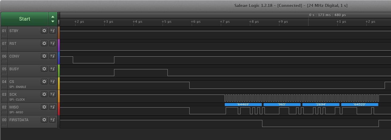
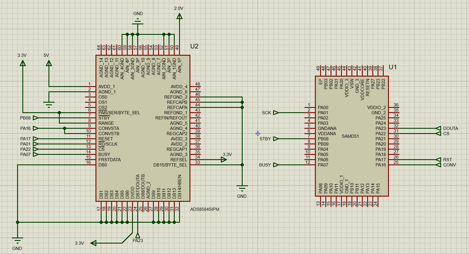
AIN_1P is connected to a static 2V output.

AI1N_1GND is connected to GND.

The rest of the ADC Input arent connected.

PAR/SER/BYTE SEL is set to HIGH.

DB15/BYTE SEL is set to LOW.

STBY and RANGE are set to HIGH.

There is a 100ms delay after STBY is set to HIGH 

REFSEL is set to HIGH.

RESET is set to HIGH, holded during 1 us and set to LOW.

There is a 25 us delay after RESET.

After that SPI is configurated as follow:

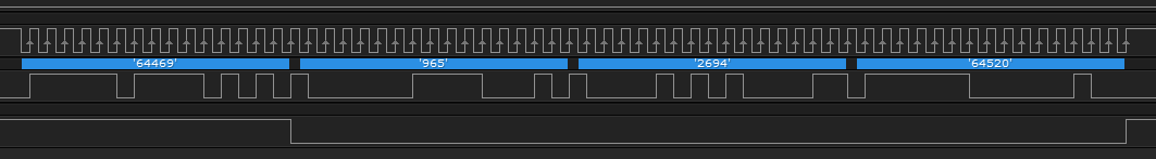
SPI Clock is set to 7.5Mhz (The SAMD51 is a 140Mhz, i tried both 15MHz and 7.5Mhz)

SPI Mode is set to MODE 3.

Only DOUTA is connected.

Any idea what am i be doing wrong?

Thanks in advance and sorry for my english!!

  • Hi Neri,

    Different processors may have different meaning for SPI mode, for example, mode 3 on ARM-based microcontroller may have an inversion of CPHA, it may be CPOL=1 and CPHA=0. For ADS8584S ADC, the conversion data is shifted out on the rising edge of the clock pulse and the data should be sampled on the falling edge of the clock pulse. Hence, please make sure you are configuring your SPI master as CPOL=1 and CPHA=1.

    From your timing, the conversion on your ADC device is working since your BUSY and FIRSTDATA signals are correct. However, the output data from ADC is Twos Complement Binary format, the MSB of the code stream should be always 0 when your input is positive 2V signal or floating. Your timing shows MSB=1 on channel 2 and 3. I think this should be a timing issue.

    Except SPI configuration, I also have a concern about your SCLK high and low time, some of your SCLK pulses show wide high time and some of them show wide low time, the expected high and low time should be 0.45 to 0.55 tSCLK, see tPH_SCLK and tPL_SCLK specifications in datasheet.

    Also, please measure the voltage on REFIO(pin 42) and REFCAPA(pin 44) and REFCAPB(pin 45).

    Lastly, your schematic will be very helpful to address the issue.

    Thanks&regards,

    Dale

  • Hi, Thanks for answering.

    Its my first time tring an ARM-based microcontroller and you were right, i was in the wrong mode. I have corrected it now... CPOL=1 and CPHA=1.

    This picture is a zoom in of the first 16 bits transmited from the ADC to the microcontroller, as you can see the CLK pulses are OK (periodic 83ns pulse) but there is a wider pulse every 8 pulses, i will try to fix that to check if that is cousing my problem.

    The REFIO voltage is 0.82V.

    REFCAPA and REFCAPB voltages are 0.72V.

    Is it possible to only sample Channel 1 and 2 of the ADC by only triggering CONVA pin?

    Thanks in advance!

  • I have fixed the SCLK timing issue..

    Zoomed out:

    Zoomed In:

  • Hi Neri,

    Your SCLK pulse looks great now. 

    You are using internal reference by pulling REFSEL high. However, based on your measurement, your reference voltage is incorrect, the internal reference voltage 2.5V should be measured on REFIO pin.

    Please use a multimeter to check if REFSEL pin is logic high. Also, are you using a pull-up resistor for REFSEL pin to DVDD? Your schematic will be very helpful to address the issue, I need to review it.

    Regards,

    Dale

  • Hi,

    The REFSEL PIN is HIGH. 

    Im using a USB to power everything, there is a Voltage Regulator (AP211K) that powers the SAMD51 with 3.3V and the ADS8584 with 5V.

    Everything else is in this poorly made schematic.

    I really hope that it helps.

    Thanks!! 

  • Hi,

    I connected all AVDD and AGND, that fixed the voltage in REFIO PIN, now i see 2.5V in my multimeter but the adc reading are still wrong..  Random numbers on each channel. 

    Im going to try another ADC, maybe i broke this one...

  • Hi Neri,

    When designing a data acquisition system with a ADC, you will have to follow the guideline and suggestions in the ADC datasheet. You can not connect only one supply pin to the power supply, also you can not connect only one ground pin to your GND and ignore all other power supply and ground pins. 

    Here are critical errors in your schematic and connections:

    1. REFCAPA and REFCAPB are internal reference amplifier output pins, you connected both of them to the GND. You force and short the reference signal to the GND, this may damage the device since it can draw a lot of current, lead to a large power dissipation and cause device burnout. These pins must be decoupled to GND through a 10-uF ceramic capacitor. See the description in page 5 of datasheet.
    2. All power supply pins should be connected to proper power supply, you only connect pin 1 and no any connection for pin 37, 38 and 48 to AVDD(5V).
    3. All ground pins should be connected to GND, you only connect pin 2 and no any connection for pin 26, 35, 40, 41, 47,53, 54, 55, 56, 61, 62, 63 and 64 to GND.

    Also,

    1. REFIN/REFOUT pin should be decoupled with REFGND (pin 43) by using a 10-uF capacitor. However, it's floating in your schematic.
    2. REFGND pin 43 should be connected to the GND, it's floating in your schematic.
    3. REGCAP1 and REGCAP2 should be decoupled separately to GND by using a 1-uF capacitor, they are floating in your schematic.
    4. Decoupling capacitors should be used on power supply pins. 
    5. When OSR is not used, suggest to connect OS0/OS1/OS2 pins to GND.

    Regards,

    Dale Li