This thread has been locked.

If you have a related question, please click the "Ask a related question" button in the top right corner. The newly created question will be automatically linked to this question.

ADS8528: Returned Data Not Consistent

Part Number: ADS8528

Hi,

I am trying to read data from an ADS8528 using SPI. Using my logic analyzer, I can see activity on the MISO pin in response to what I am sending but I am unable to make sense of the data.

I have tried to read the config register back by setting bit 30 high and then initiating a read but that doesn't give the value that I just wrote to the config register as I would expect.

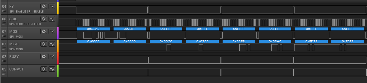
I think I would expect the values after the first two CONVST/BUSY cycles to be the Config register based on setting Bit 30 high. I then would expect the third (and ensuing) reads to be A/D values. Does that sound right?

I saw another post on E2E (here) that said they were able to tell that the configuration was working because they could see the REFIO pin go from 2.5V to 3.0V. Unfortunately, when I try to measure it with my Fluke, it just shows voltage dissipating (presumably due to the capacitor to ground).

I'm struggling to make sense of what I think the datasheet is saying vs what I'm actually seeing but I'm prepared for the problem to be my ignorance.

Thanks,

Jim

  • Some further information.

    When I try to just read data (instead of trying to read the config register first), the BUSY bit always goes back high in the middle of reading the 4th word. See picture below. I switched to 32-bit reads/writes to see if that would make a difference.

    I can't find anything about that in the datasheet. Maybe it is a clue to what I am doing wrong?

    Thanks,

    Jim

  • Hi Jim,

    Thanks for your post.

    Testing the REFIO pin is a good approach. The voltage should hold constant after power-up, and any changes to the reference value should be readily apparent. You can either toggle CONFIG [13] to switch between 2.5 V and 3 V, or write any value between 000h and 3FF to CONFIG[9:0] to scale the reference output. Do either of those options show a change in the REFIO voltage?

    Can you confirm how the hardware mode pins are set? Specifically pin 41 (HWn/SW)?

    Best regards,

  • Hi Ryan,

    Thanks for your response.

    I have made some progress here and appreciate your input.

    I have found and resolved a few issues:

    1) I found here, that I needed to be sending 0x00's instead of 0xFF's when I was reading values. This resolved the issue where the BUSY bit was going back high. I've always thought 0xFF's was the standard and didn't realize that was a problem.

    2) I didn't have C15 set to 1 in my  configuration register. This was a silly mistake by me. That is why my REFIO pin wasn't stable. Once I set that to one, I have predictable control of the REFIO pin (C13 low and REFDAC at 3FF is 2.506V; C13 high and REFDAC at 1FF is 1.507V, etc).

    3) My logic analyzer was another issue. I didn't have it properly grounded so that caused the config read value to appear wrong and the A/D values to seem to be totally out of range. The config register looks mostly accurate and the A/D values look more reasonable.

    So, it looks like I am writing to the configuration register successfully and getting reasonable values for the A/D.

    The only remaining issue is that there seems to be some excessive (local) variation in the A/D values from reading to reading. One of the pins is at 1.648V  equal resistor divider on 3.3V line). When I'm reading it, it is varying from 1.16V to 1.94V. I'll keep looking into that and report back what I find.

    Thanks,

    Jim

  • Hi Jim,

    Nice to hear that you made progress on this! 

    Some of our devices do allow for either 0x00 or 0xFF as a no-operation command, but not the ADS8528.

    The conversion error you're now seeing could be related to the input drive circuit or perhaps noise coupling through the AGND. Is there just a resistor divider on the input pin? Adequate drive strength is required to deliver charge to the internal sampling capacitors and to settle the input voltage between conversions. You will likely need a buffer, followed by an R-C filter to deliver this charge.

    Best regards,

  • Hi Ryan,

    I am sending a snip of the schematic for this to show how the resistor divider drives the spare pin and how the 7 actual sensors work.

    Any thoughts?

    Thanks,
    Jim

  • Got it!

    We didn't have REFAN, REFBN, REFCN and REFDN grounded. Things look solid now.

    Thanks for your input!

    Jim

  • Hi Jim,

    Glad you worked it out. I looked a the schematic briefly yesterday evening but missed that detail. Good catch!

    Let us know if you run into any other issues.

    Best regards,