This thread has been locked.

If you have a related question, please click the "Ask a related question" button in the top right corner. The newly created question will be automatically linked to this question.

ADS1298: reducing converter noise - decoupling issues

Part Number: ADS1298

I am looking at ways of reducing the noise on my ADS1298 implementation.

Board is configured with decoupling capacitors as per datasheet but I am getting a RMS Noise of between 50 and 100µV when I place the device in High Resolution Mode DR Bits 010 (8000 SPS).

The data sheet Table 1. indicates that a level of 12.4µV ought to be possible. Any idea on areas I can improve?

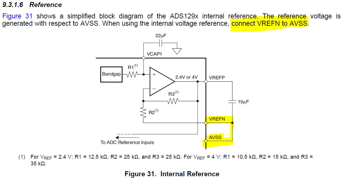
In my configuration I am using bipolar supplies (±2.5V). I see that VCAP1 which decouples the reference voltage ought to be connected to Vss. If this is the case then don't I lose the PSRR of the device since noise will be coupled in from the power rail straight onto the reference voltage? Wouldn't I be better to connect to GND ?

Are there recommendations on the ESR of the capacitors that I should be using?

  • Hi Phil,

    Keep in mind that the noise specifications in the data sheet are measured with an internal input-short condition. It is realistic to expect external noise from your signal source and power supplies couple into the signal chain and add to that total noise.

    Depending on the nature of the noise, reducing the ADC bandwidth can help filter more noise. This is done by reducing the data rate. Antialiasing filters can be added to the inputs, but these are intended to filter higher frequency signals, not those within the ADC bandwidth itself.

    VCAP1 is the bandgap voltage used to generate the reference voltage. When the ADCs sample, they compare the differential input to the differential reference voltage (REFP - REFN). REFN should also be connected to AVSS, so VCAP1 should be decoupled to AVSS as well.

    There is not a recommendation for ESR for bypass capacitors. For signal chain capacitors, use NP0/C0G types.

    Best regards,

  • I was using the internal short too - this doesn't include external generated noise from the resistors/filters in the front end so external filters wouldn't help.

    Section 9.3.1.4 Analog Input recommends "holding INN to common mode voltage, preferably at midsupply." since I have bipolar supplies I have kept this at analog GND which is half way between AVSS and AVDD.

    You are suggesting that REFN ought to be connected to AVSS (-2.5V in my system) ?

  • Hi Phil,

    Thanks for clarifying. The internal input-short configuration automatically connects both PGA inputs to mid-supply, so this setup is fine.

    Yes, REFN must be connected to -2.5 V. Please refer to Figure 31 in the data sheet.

    I realize that this figure shows VCAP1 decoupled to ground. Technically, we want all four VCAPx pins to be decoupled to AVSS.

    Please let me know if this resolves the noise issue.

    Best regards,

  • hi Ryan,

    I misunderstood what you meant by reference - I thought that you were talking about the negative part of each Analog Input. These I have connected to GND.

    My VREFN is connected as per Fig 107 in data sheet with a 10µF and 100nF capacitors to VREFP and direction connection to AVSS.

  • Hi Phil, 

    Are you still working on this issue? I know we have a couple other threads going in parallel.

    Regards,

  • Still working on this. Perhaps direct message would be better format at the moment rather than forum.

  • Hi Phil - I will contact you offline at the email address in your profile.

    Regards,