This thread has been locked.

If you have a related question, please click the "Ask a related question" button in the top right corner. The newly created question will be automatically linked to this question.

ADS131M08: Datasheet clarification for clocking the ADC

Part Number: ADS131M08

Hello,

Under section 8.3.5 of the datasheet it talk about how to clock the ADC, I am getting mixed interpretations on how it is stated and I would like to ask some help for clarifications.

The first sentence of the paragraph says 

 "The master clock can either be sourced externally to the CLKIN pin or generated internally using the onboard oscillator that requires a crystal connected between the XTAL and XTAL2 pins

The second part of the sentence sounds contradicting to me, there is an onboard oscillator but would still need an external crystal oscillator? What would be the purpose of the internal oscillator if you need to have a external crystal oscillator anyway?

In the second to the last statement of that paragraph

"When not using the internal oscillator, turn it off to save power"

So there is an internal oscillator?? 

On the Clock Register the bit responsible for the the clock are these two 

7          XTAL_DIS            R/W           0b             Crystal oscillator disable          0b = Enabled (default)          1b = Disabled

6          EXTREF_EN       R/W            0b             External reference enable       0b = Disabled (default)          1b = Enabled

So if i use a Microcontroller GPIO i have to disable(1b) XTAL_DIS, and enable(1b) EXTREF_EN. (Quite confusing for me because it could interpreted as to "enable (0b)" the the crystall oscillator "disable"  thus disabling the crystal oscillator. Also what would happen if you forgot to disable the Crystal Oscillator , while you use an external reference, wwould it operate normally but just waste power?

Last that i would need clarification is 

The development board seems to not synchronize the SPI SCLK as opposed to what the datasheet says.

DataSheet: "For optimal performance, the modulator sampling clock must be synchronous with the serial data clock SCLK. The modulator sampling clock is derived from the master clock which means the master clock should be synchronous with the SCLK."

EVM DataSheet: "The ADS131M08 requires a continuous, free-running external master clock at the CLKIN pin for normal operation. The onboard complementary metal oxide semiconductor (CMOS) crystal oscillator (Y1) provides the nominal 8.192-MHz clock frequency used in the high-resolution (HR) mode of the device."


Does this mean that its not as critical to synchronize the SPI SCLK and CLKIN ??

Thank you.

  • Rykilth,


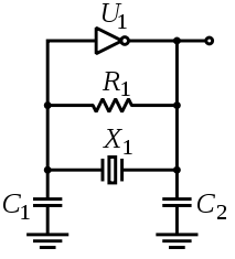
    First, the master clock can come from a clock from an external source, or the device can use an external crystal similar to a Pierce Oscillator, with the inverter in contained in the device, similar to the figure below. I believe that this is a leftover text from another similar device which does have an internal oscillator.

    Then with crystal oscillator, you want to disable it to save power. If the inverter is active, then the crystal will continue to oscillate. That oscillation will drive part of the clock tree in the device. Again there is no internal oscillator in this device. I'll see if I can have that changed in the datasheet.

    Going onto the Clock Register settings:
    For the XTAL_DIS bit, you can read this as Crystal Oscillator Enable, active low. So 0=Oscillator Enabled, 1=Oscillator Disabled.
    For EXTREF_EN bit, read this as external reference enable, so 0=External Reference Disabled, 1=External Reference Enabled.

    Finally, for some of our wide-bandwidth devices, we've recommended that the SPI_CLK and the CLKIN are synchronized to get the best SNR performance. However, not having them synchronous isn't required. It may affect the SNR by a couple of dB. However, this device isn't really designed to have the same input bandwidth. In my measurements with it, the noise performance is very close to the values listed in Table 1 and 2 of the datasheet.

    Hopefully, that clears up your questions about the device. If you have any other questions, let me know.


    Joseph Wu

  • Hi Joseph,

    Thank you very much for you reply! 

    A quick follow up question, i could not find a section on the datasheet on how the crystal should be setup. If i understand correctly in the circuit you have shown, R1 and U1 are inside the IC. What would the recommended capacitor value be?

    So placing a fix Crystal on X1 will give me access to only 1 power mode. If i want access to the other modes i should do it like how the development board does it. Correct me if im wrong but the circuit look like this?

    Rykilth Knox Concepcion

  • Rykilth,


    The capacitors connected to the crystal are the load capacitors for the crystal. This will vary from crystal to crystal, so you would determine that from the crystal itself. Note that if you do select a crystal, the load capacitance will also vary with the parasitic capacitance in the layout. In my experience, the parasitic capacitance is a larger contributor than you might expect. Without considering the parasitic capacitance, the crystal may not startup. Crystal manufacturers will have some documentation how to use the crystal and calculating the load capacitance.

    The way you have the crystal connected in the schematic will not work. The inverter connection should be direct, and the oscillator output is too small to be sent directly to a standard logic gate and must be sent through other circuitry to be used (that's what happens inside the device).

    If you want to use multiple power modes, you would not use a crystal, you would use an oscillator. For an oscillator, it's basically a crystal with the inverter, load capacitance, and conditioning circuitry. The output of the oscillator gives a digital clock. If you want to use this, just copy the oscillator from the ADS131M08EVM. The clock dividers show in you part of the schematic are the same.


    Joseph Wu

  • Hi Joseph,

    Oh ! I apologize for asking so quickly, i did not notice that there was a part list and schematics at the very end of the datasheet. 

    Thank you very much for your responses.

    Have a great day!

    Rykilth Knox Concepcion