This thread has been locked.

If you have a related question, please click the "Ask a related question" button in the top right corner. The newly created question will be automatically linked to this question.

ADS124S08: Power frequency suppression

Part Number: ADS124S08

Hi Team,

The customer is experiencing below issue and needs your help.

  1. If the ADC Data rate is set to 10sps, is the maximum SPI output data rate 10sps?
  2. If the ADC Data rate is set to 10sps, choose 6-channel data acquisition, how to ensure that the 6-channel alternating data acquisition rate (using Low-Latency Filter filtering) and ADC Data rate are synchronized?eg: The output channel data is output in the order of ch1, ch2, ch3, ch4, ch5, ch6, ch1, ch2, ch3, ch4, and ensure that the output is synchronized with the ADC Data rate.
  3. If the ADC Data rate is set to 10sps, select 6 channels of data for alternate acquisition (using Low-Latency Filter), can power frequency noise be suppressed for each channel?

Thanks,

Annie

  • Hi Annie,

    See my responses below.

    Best regards,

    Bob B

    Annie Liu said:

    Part Number: ADS124S08

    Hi Team,

    The customer is experiencing below issue and needs your help.

    1. If the ADC Data rate is set to 10sps, is the maximum SPI output data rate 10sps? [Bob] I'm not totally sure what is being asked here, but if the data rate is set to 10sps, the new conversion data will be available every 100ms (10Hz which equals 10sps).  The data should be read out of the ADS124S08 completely before the next conversion result has completed.  So the SPI SCLK frequency must be fast enough to retrieve all 24-bits of data between each conversion period.
    2. If the ADC Data rate is set to 10sps, choose 6-channel data acquisition, how to ensure that the 6-channel alternating data acquisition rate (using Low-Latency Filter filtering) and ADC Data rate are synchronized?eg: The output channel data is output in the order of ch1, ch2, ch3, ch4, ch5, ch6, ch1, ch2, ch3, ch4, and ensure that the output is synchronized with the ADC Data rate. [Bob] The customer would need to keep track of the sequence in firmware.  There are several ways to accomplish this with the simplest being a loop.  If single-shot conversion is used:
      1. You setup mux for ch1
      2. Start the conversion
      3. Wait for the conversion to end
      4. Read the result and save the value to a channel data array
      5. Setup the next channel to be converted
      6. Loop to b
    3. If the ADC Data rate is set to 10sps, select 6 channels of data for alternate acquisition (using Low-Latency Filter), can power frequency noise be suppressed for each channel? [Bob] Yes, the filter response will follow Figure 56 on page 39 of the ADS124S08 datasheet.

    Thanks,

    Annie

  • Hi Bob B, 

    Customer updated his problem again.

    ADS124S08 signal input circuit is consistent with TI reference design. AINP and AINN use 10M resistors to connect to 3.3V power and ground respectively. When measuring signals:

    1. When the thermocouple is connected, the bias voltage of the thermocouple signal input terminal is 1.14V (not the ideal 1.65V).

    2. When the thermocouple is disconnected, measure the voltage of VINP (VINP is connected to 3.3V through a 10M resistor) and it is 1.73V (not ideal 3.3V).

    Customer would like to know is there any abnormality?

    3. Thermocouple signal, single channel continuous sampling, program configuration:

    • Enable PGA, PAG gain is set to 4 (final signal gain: 32 X 4)
    • Adopt SIN3 and Global Chop Mode, data output rate is 20sps, other configurations are default

    The final data measurement result can only maintain the accuracy of mV level, but cannot meet the accuracy of 10uV level. May I know is there a problem with the ADC configuration?

    Customer attached application circuit diagram6888.Thermocouple.pdf

    Thanks,\

    Annie

  • Hi Annie,

    There appears to be some significant leakage current.  The leakage current can come from several sources:

    • TVS diodes
    • ADC leakage and bias currents
    • Flux residue on PCB and input current path

    The important question at this point is whether all of the TC inputs act the same way or if only some of the inputs are showing this issue?

    The next question to be answered is if the voltage levels remain the same in both the condition where the input mux has selected the input channels and a conversion is taking place, compared to the condition where the inputs are not selected?

    As to the actual voltages given for the various conditions (TC connected and TC unconnected) the currents don't match up.  Normally I would expect to see about 165nA of current with the TC connected.  The voltage drop across the pull-down resistor is 1.14V which equates to 114nA instead of 165nA.  This would equate to a leakage of about 51nA.  If the TVS diodes are leaking, then this would be considerable leakage for the diode part numbers shown in the schematic.  If different TVS diodes were used, then I've seen leakage at 1uA or even more.  So it would be good to verify if the TVS diodes are the issue and this could be checked by simply removing them.

    Where I have a calculation problem is where the TC is disconnected and the voltage at the input is 1.75V.  This would mean a considerable amount of current flowing through the pull-up resistor and the leakage much higher at this pin compared to the case when the TC is connected.  So this condition doesn't make much sense to me.  For further analysis it would be very helpful to know the answers to the questions I proposed above.

    Best regards,

    Bob B

  • Hi Bob,

    1. all of the TC inputs act the same way

    2. Remove the circuit TVS tube, the measurement result has not changed. Didn't select the channel, TC is disconnected, the measured voltage is 1.732V. Select the channel to start conversion, TC is disconnected, the measured voltage is 1.71V.

    And

    • (Remove TVS in the circuit) Use a multimeter to measure the pull-up and pull-down 10M resistance value of TC input terminal is 6.45M;
    • Select a channel, disconnect the differential signal line (disconnect the signal line connected to the chip), re-measure 10M resistance value, the measurement result is normal: 10M

    Thanks,

    Annie

  • Hi Annie,

    This is a very interesting situation and a bit difficult for me to troubleshoot.  For there to be this much leakage current there would need to be a voltage difference somewhere that would cause the current to flow.  For example, if VBIAS were accidentally enabled you would see a current flowing from the source of the pullup resistor to the 1.65V voltage bias.

    Another situation where the current can flow is if the pullup source voltage is 5V, but the AVDD supply is less than 5V.  However this doesn't seem likely given the layout.

    The last thing I can think of is if an input is connected to a power supply as opposed to an actual TC where the voltage potential is higher than the analog supply.

    So there is significant troubleshooting required to find the root issue.

    Best regards,

    Bob B

  • Hi Bob B,

    Customer removed the 10M resistor and used paranoia inside the chip, the measurement result wasn't satisfactory. (The input is a standard signal source, the larger the input signal, the greater the sampling error value. eg. 1mv signal, measurement result is 1.13mv, 10mv signal, measurement result is 9.3mv) The measurement results are similar to the use of an external bias voltage.

    Software execution:

    ①Reset the chip->②Register select channel->③Enable internal gain, configure 4 times gain (final gain result 32 X 4=128)->④Configure data output rate to 20sps, start SIN3 filter and global chopping- >⑤Enable continuous conversion, the remaining registers are the default configuration. Is there a problem with the ADC sampling configuration?

    The leakage current path may have been found. The test method is as follows:

    Disconnect the channel of the input signal channel ADC (the disconnection position is between the passive filter circuit and the ADC), and the measured TC disconnection voltage is 1.73V, which can indicate that the leakage current does not flow into the ADC. How does this lead to inaccurate ADC sampling? If it is not a hardware problem, is there any problem with the above software configuration?

    Thanks,

    Annie

  • Hi Annie,

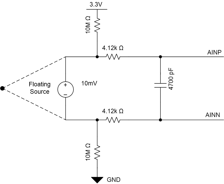
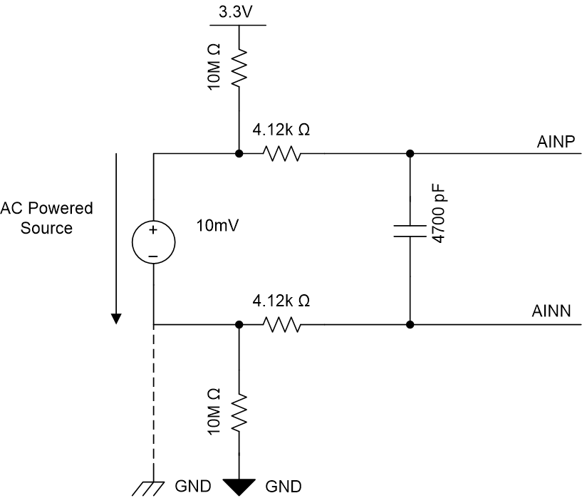
    This is very helpful information.  If you have a standard external voltage source connected to the analog inputs, this source most likely is connected to a standard AC power outlet.  The relationship of the ground of the signal source and the ground of the ADC plays an important role in how the actual value of the input voltage is established at the ADC.  I have seen as much as 40V difference in common-mode between sources.  This is due to the AC source converted to a DC source.  So the + and - outputs of the voltage source really need to be floating with respect to the ADC TC input.  This is best accomplished with a battery source.  This is the method often used with TC calibrators. 

    An actual TC is an independent floating voltage source where the junction of the two dissimilar metals create a potential.  The TC voltage must be within the input range of the ADC and that is why the pull-up and pull-down resistors accomplish by placing the TC voltage at approximately (AVDD-AVSS)/2. 

    The input restriction for the ADC is related to the PGA setting.  For a gain of 32, the input is restricted to a minimum absolute voltage of AVSS + 0.15V + 15.5*|VinMax| and a maximum input voltage of AVDD - 0.15V - 15.5*|VinMax|.  Lets say the maximum input voltage (VinMax) would be 20mV for a K-type TC.  This would require that the absolute input voltage be between 2.84V and 0.46V.

    1.73V is within this range, but 0V is not.  How can there be 0V on an input?  This is where the issue of the AC powered DC source can become an issue.  If there is a pathway where current will sink through the external DC source, the input at AINN can become 0V.  A 0V input using the PGA will create an error as the PGA cannot drive to the rail.  The larger the input signal the worse the error will appear and the error will be non-linear.

    There will most likely be some small leakage source, but you want to minimize the leakage and make sure that the testing methods used follow the design of the circuit.

    Best regards,

    Bob B