This thread has been locked.

If you have a related question, please click the "Ask a related question" button in the top right corner. The newly created question will be automatically linked to this question.

ADS8568: Output data format and input signal conditioning

Part Number: ADS8568
Other Parts Discussed in Thread: ADS8688A, OPA209

Hey everyone!

I've looked at the ads8568 briefly in the past but now need to implement it in a design.

Concerning the output data format in serial mode. If I have this correctly the format looks like it uses spi or qspi depending on how many output pins are chosen. I'm not sure whether I'm analyzing the serial timing diagrams incorrectly and whether another peripheral would better suit it?

Concerning the input signal, It seems that the input is a single ended true bipolar and thus the full range runs over a the span from a negative to positive reference value. My input signal however is Unipolar and DC. It will vary between 0 to 5V, I thus want to know whether there is a signal conditioning I can apply to get my input signal to span the whole bipolar range. So a conversion where the the input signal is conditioned from say 0 -> 5V to -5V -> 5V. 

some key points of the signal will then be

original -> new 

0V will become -5

2.5V will become 0V

5V will be 5V

Thanks in advance for any help!

  • One thing to note is that I'll be daisy chaining the 3 Devices to obtain 24 simultaneous sampling channels 

  • Hi PieterT,

    The serial mode on ADS8568 is a standard SPI interface if only one SDO is chosen, including SCLK, SDI, SDO_A and  /FS&/CS. The SCLK frequency should be limited to 0.1MHz~45MHz. When the serial interface is selected, the ADC can work on either Hardware mode without programming internal register through SDI or Software mode with SDI. Also, more serial data output ports (SDO_B,SDO_C and SDO_D) can be selected and configured to achieve a higher sampling rate if your microcontroller or CPU has a flexibility to receive the data from them.

    When multiple ADS8568 ADCs are used in daisy-chain mode, the maximum sampling rate on each ADC will be limited more because a same serial interface is shared by these ADCs.

    Regarding your question about input, yes, ADS8568 was designed for high voltage bipolar signal acquisition application and it supports only +/-5V and +/-10V input, or +/-12V if a 3V reference voltage is applied. A signal conditioning circuit on ADC input is required for a signal from 0-5V to +/-5V to use the full scale range of ADC. Otherwise, you will lose half of dynamic range on this ADC. Also, a higher bandwidth amplifier on each channel is usually required to drive ADS8568 working at a higher sampling rate since this ADC has a common switch-capacitor input structure.

    Is the simultaneous sampling really required in your application? if not, ADS8688A can be used. ADS8688A has a 0V~5.12V input range which is one of 9 input ranges supported by this ADC. Also, ADS8688A is a 16-bit, 8-ch SAR ADC with integrated analog front-end (AFE) including PGA, LPF and ADC driver which usually eliminate the requirement of designing a driving amplifier on each channel. 

    Best regards,

    Dale Li

  • Hi Dale Li,

    Thanks for the detailed reply!

    "The serial mode on ADS8568 is a standard SPI interface if only one SDO is chosen, including SCLK, SDI, SDO_A and  /FS&/CS. The SCLK frequency should be limited to 0.1MHz~45MHz. When the serial interface is selected, the ADC can work on either Hardware mode without programming internal register through SDI or Software mode with SDI. Also, more serial data output ports (SDO_B,SDO_C and SDO_D) can be selected and configured to achieve a higher sampling rate if your microcontroller or CPU has a flexibility to receive the data from them."

    If the additional data outputs are used (SDO_B,SDO_C and SDO_D) then I'm assuming QSPI can be used? just want to double check on this.

    "Regarding your question about input, yes, ADS8568 was designed for high voltage bipolar signal acquisition application and it supports only +/-5V and +/-10V input, or +/-12V if a 3V reference voltage is applied. A signal conditioning circuit on ADC input is required for a signal from 0-5V to +/-5V to use the full scale range of ADC. Otherwise, you will lose half of dynamic range on this ADC. Also, a higher bandwidth amplifier on each channel is usually required to drive ADS8568 working at a higher sampling rate since this ADC has a common switch-capacitor input structure."

    Do you have any recommendations for the signal conditioning circuit that I can use? I've been struggling to find something to properly condition the signal.

    "Is the simultaneous sampling really required in your application? if not, ADS8688A can be used. ADS8688A has a 0V~5.12V input range which is one of 9 input ranges supported by this ADC. Also, ADS8688A is a 16-bit, 8-ch SAR ADC with integrated analog front-end (AFE) including PGA, LPF and ADC driver which usually eliminate the requirement of designing a driving amplifier on each channel. "


    I wish I didnt need simultaneous sampling as that would really open up my options, but sadly I definetly need simultaneous sampling.

  • Hi PieterT,

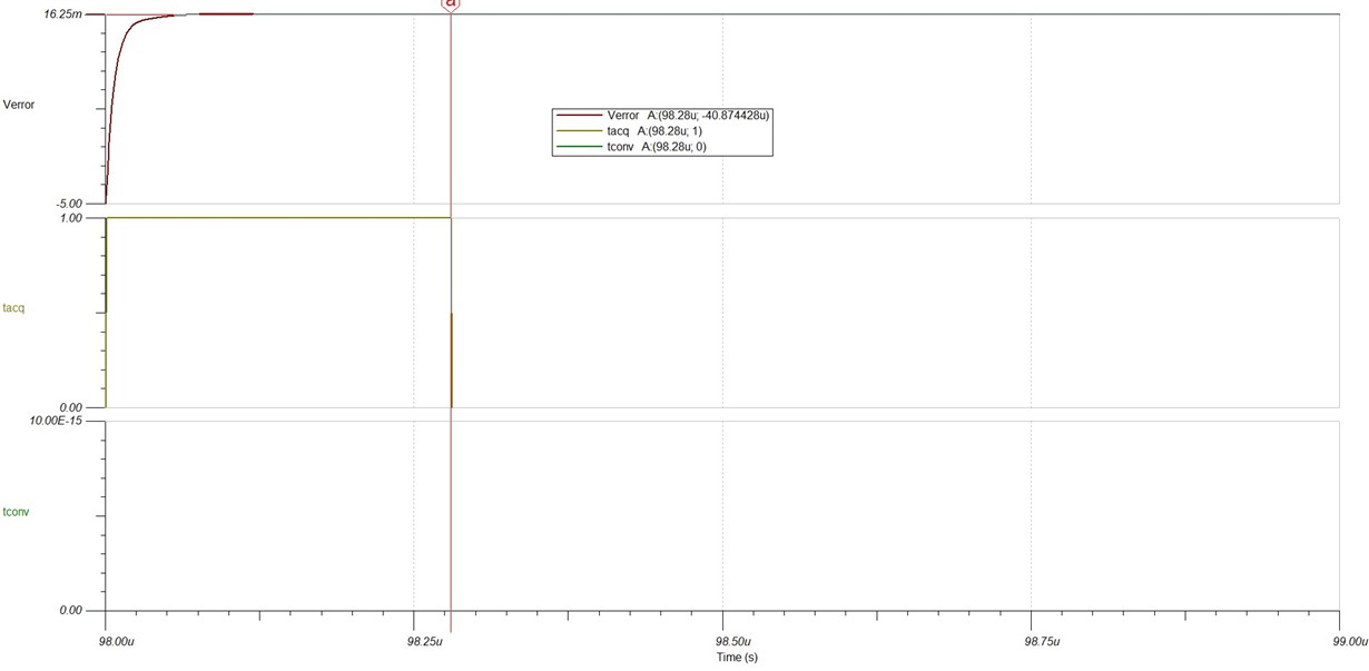
    My recommendation circuit and simulation result are shown in 1st picture below, which is using a Non-Inverting Op Amp with an Inverting Vref. The front-end circuit is used to drive ADS8568 which is a switched-capacitor input structure SAR ADC, also this circuit is used for signal conditioning from 0-5V to -5V~+5V to match the ADC's input range. OPA209 high BW Op Amp in the circuit is able to drive ADS8568 to work at highest sampling rate, the associated simulation result to check settling error is shown in 2nd picture. The 40uV settling error is less than 0.5LSB(76Uv) and meets the signal settling requirement. I attached the simulation source file here that can be opened in TI-TINA software, for your reference.

    /cfs-file/__key/communityserver-discussions-components-files/73/ADS8568-Non-Inverting-Op-Amp-with-Inverting-Vref.zip

    There is another circuit shown below can be used for your application as well, which is using a Inverting Op Amp with a Non-Inverting Vref. Note that the key advantage to use 1st circuit above is to have higher input impedance.

    For more information about the simulation for ADCs, please refer to TI Precision Labs - ADCs.

    QSPI (Quad SPI) should be able to interface with ADS8568, however the parameters and function of QSPI interface peripheral may vary from manufacturer to manufacturer, you will have to check if they can meet the timing requirements specified in Figure 1 and tables for associated timing parameters in the datasheet.

    Best regards,

    Dale Li