This thread has been locked.

If you have a related question, please click the "Ask a related question" button in the top right corner. The newly created question will be automatically linked to this question.

ADS8168: Not responding to write requests

Part Number: ADS8168

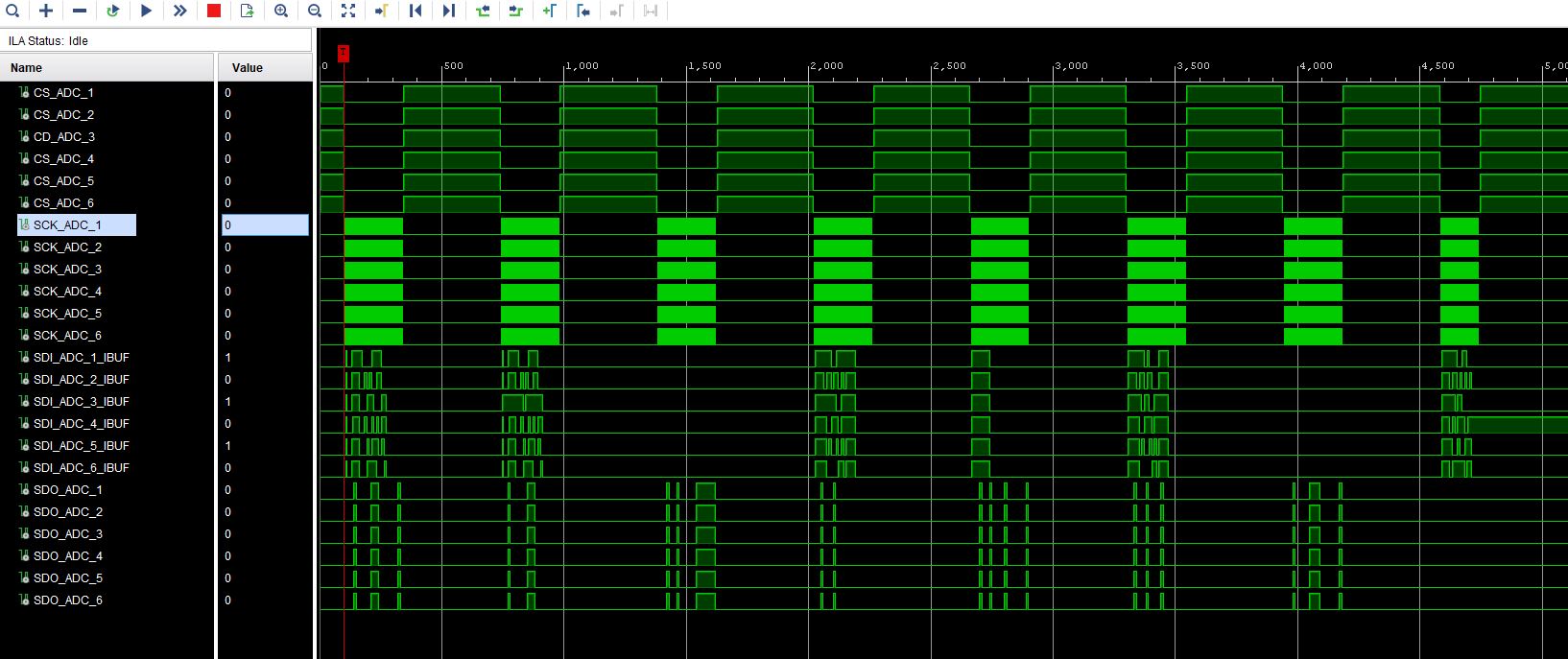
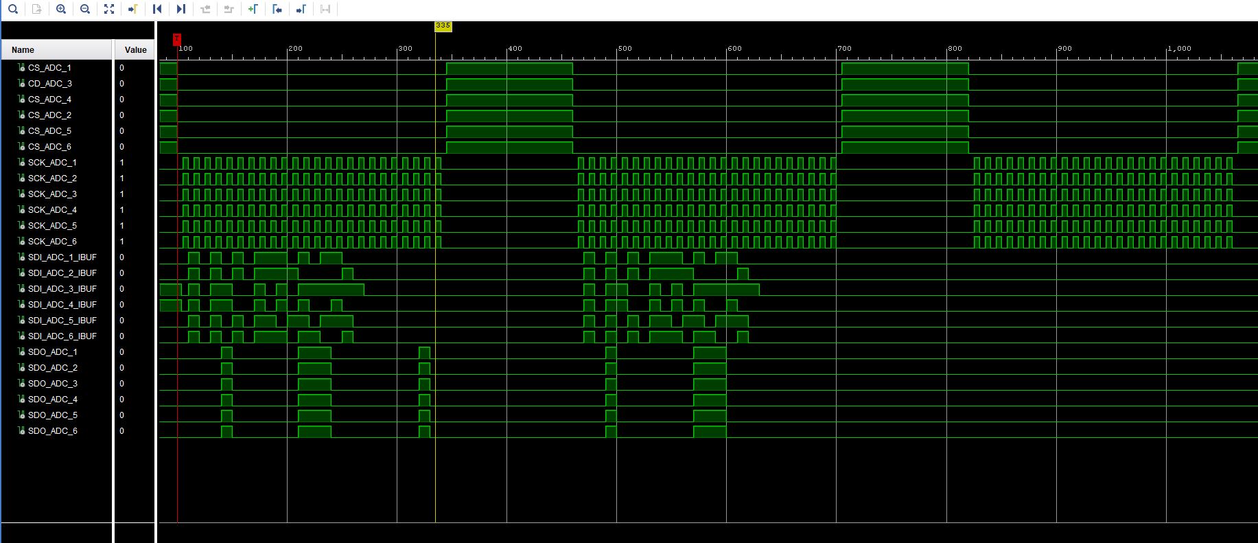
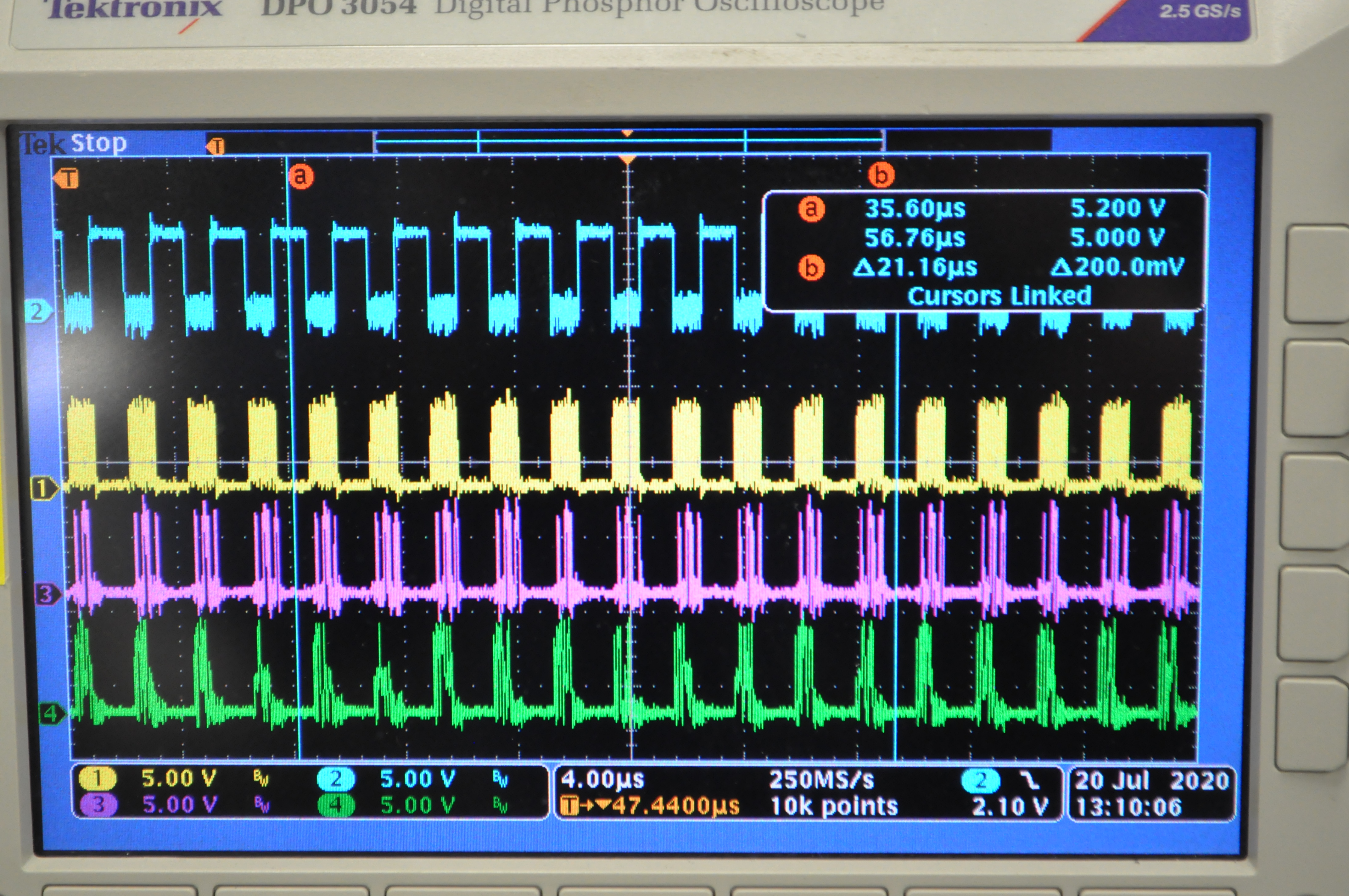
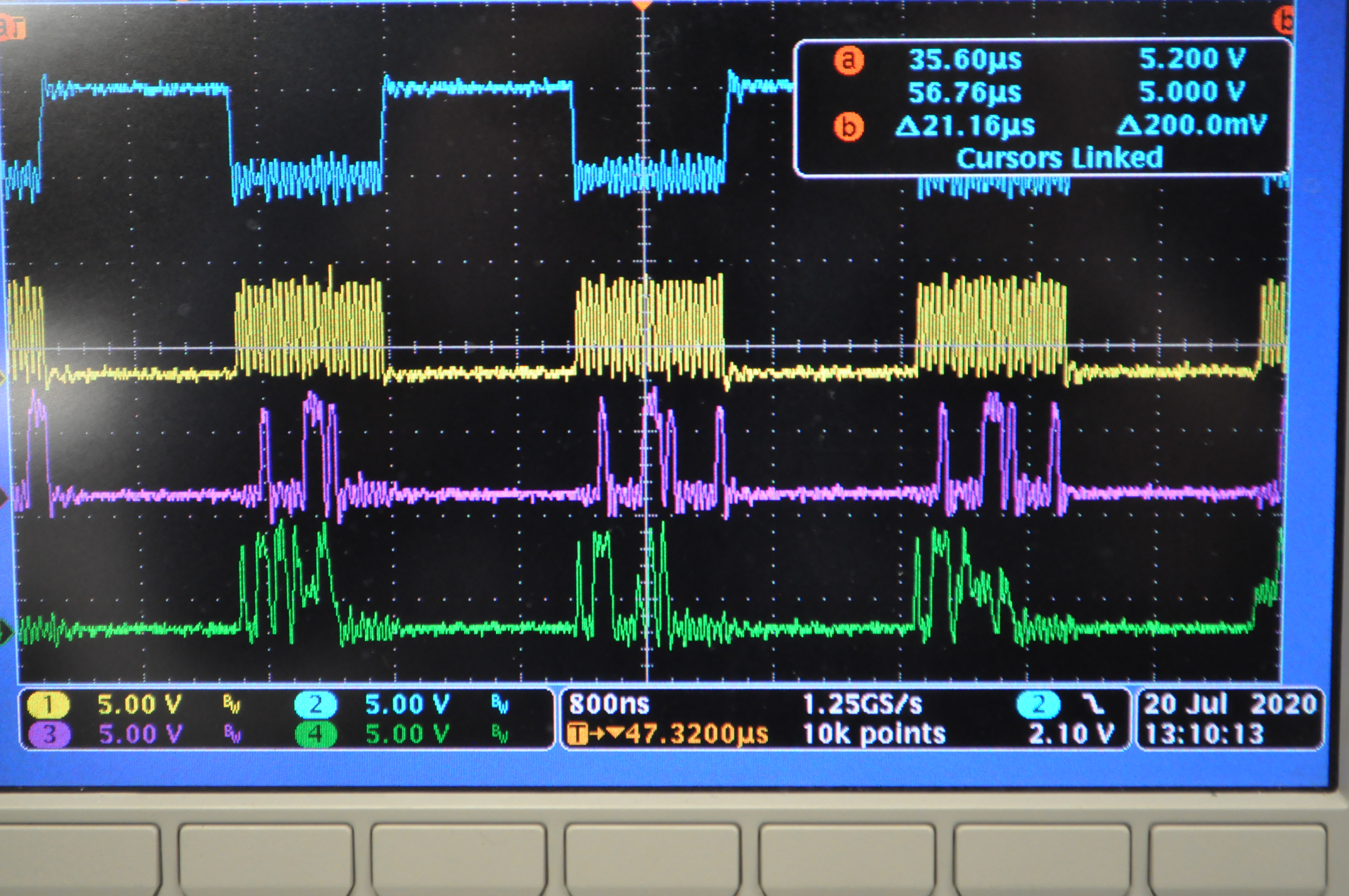
I have 6 of these ADCs on one board and when I issue write requests to put all of the devices into auto sequence configuration on all channels, they never take effect. Read requests respond with default value after issuing the write requests. 

Write : Address: 0x1C Data: 0x02 (24-bit 0x08_1C_02) To configure into auto sequence

Read : Address: 0x1C Data: 0x00 (24-bit 0x10_1C_00) Readback write, This yields data of 0x00 

Write : Address: 0x80 Data: 0xFF (24-bit 0x08_80_FF) To enable all 8 channels 

Read : Address: 0x80 Data: 0x00 (24-bit 0x10_80_00) Readback write, This yields default data of 0xFF 

Write : Address: 0x82 Data: 0x01 (24-bit 0x08_82_01) To enable Auto Repeat

Read : Address: 0x82 Data: 0x00 (24-bit 0x10_82_00) Readback write, This yields data of 0x00

Write : Address: 0x1E Data: 0x01 (24-bit 0x08_1E_01) To start the sequence

After completing this sequence, the devices all continue to just send back Channel 0 Data, since its still in manual mode and I did not change Channel ID Address 0x1D.

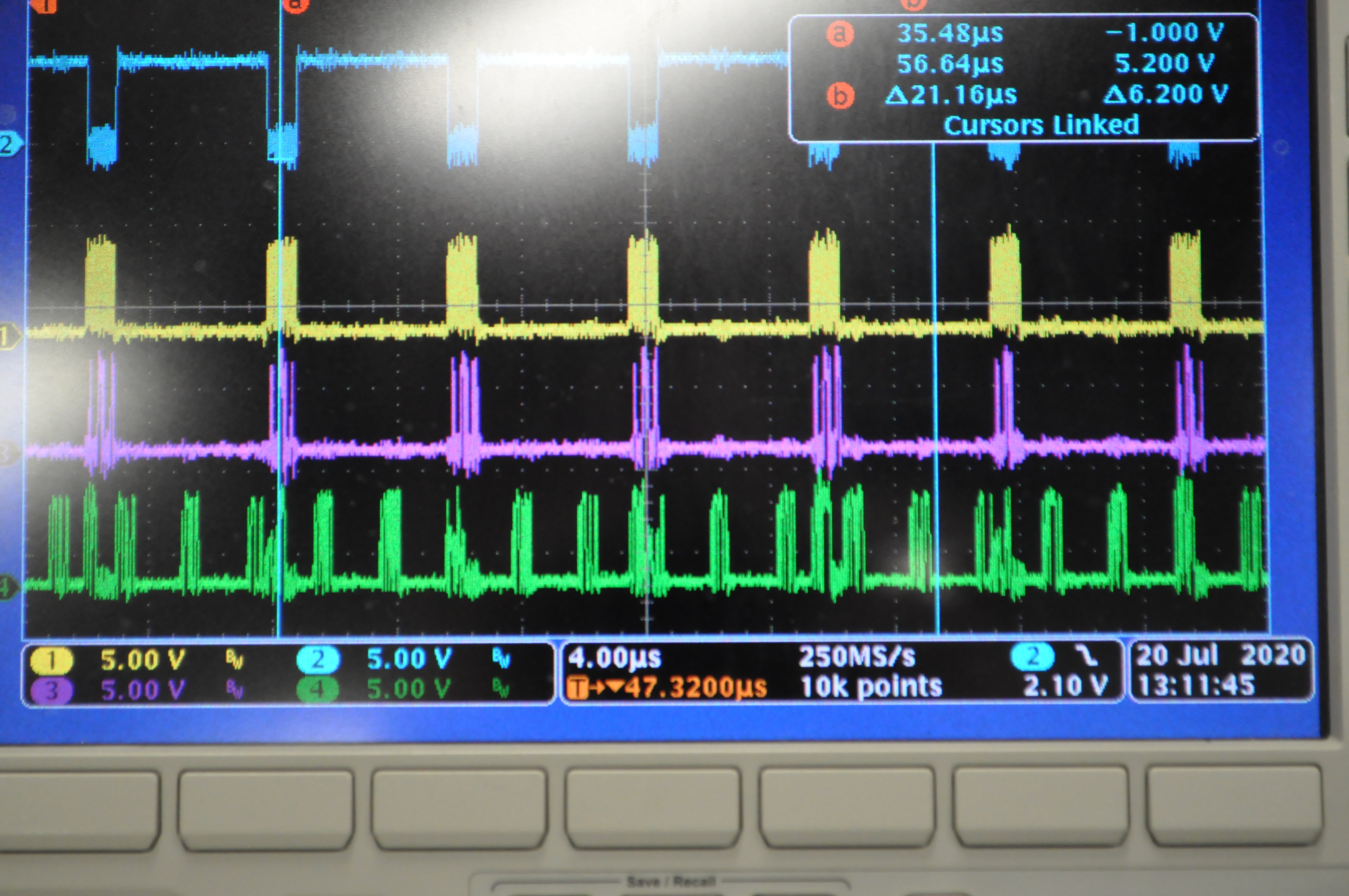
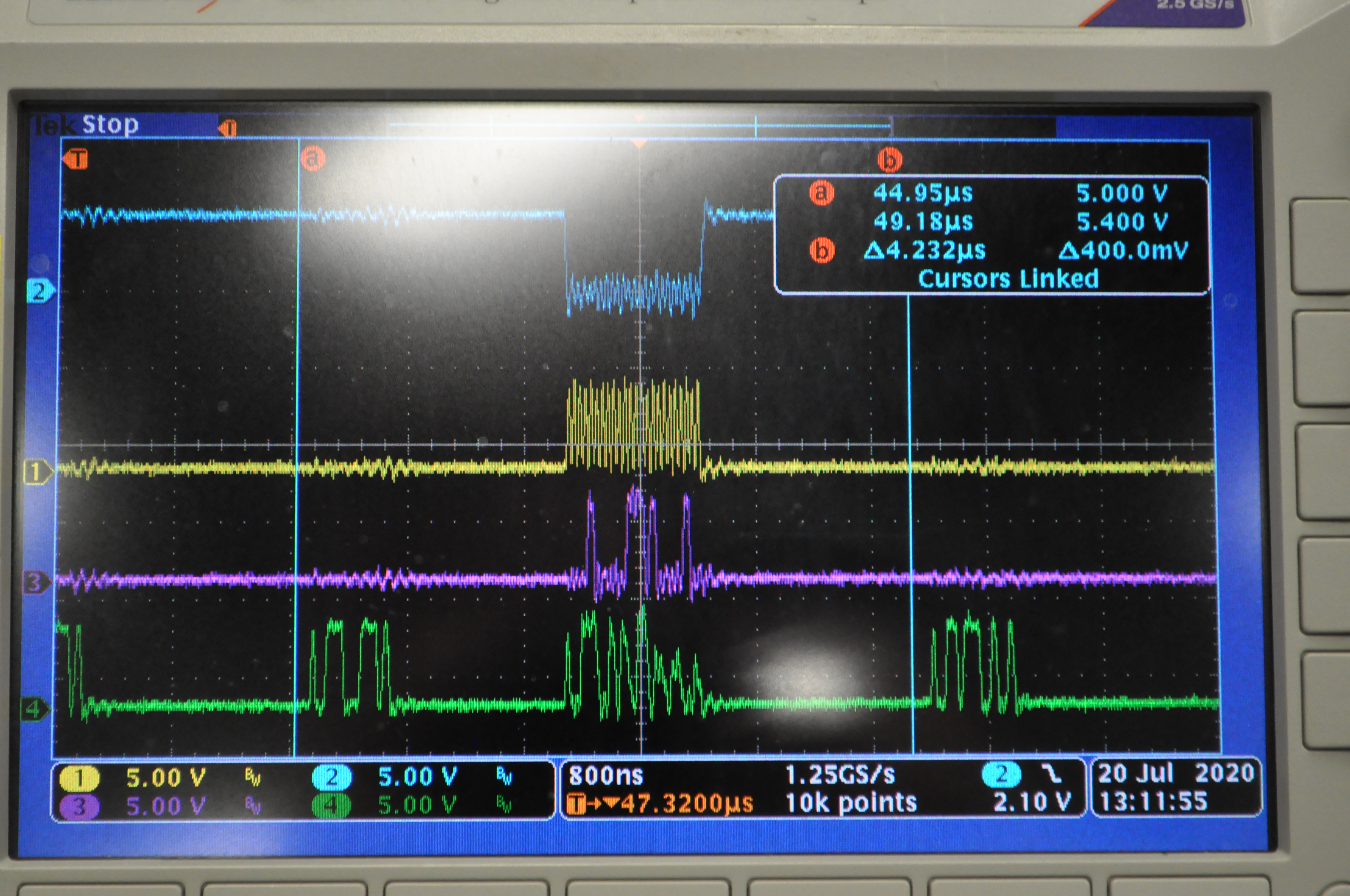
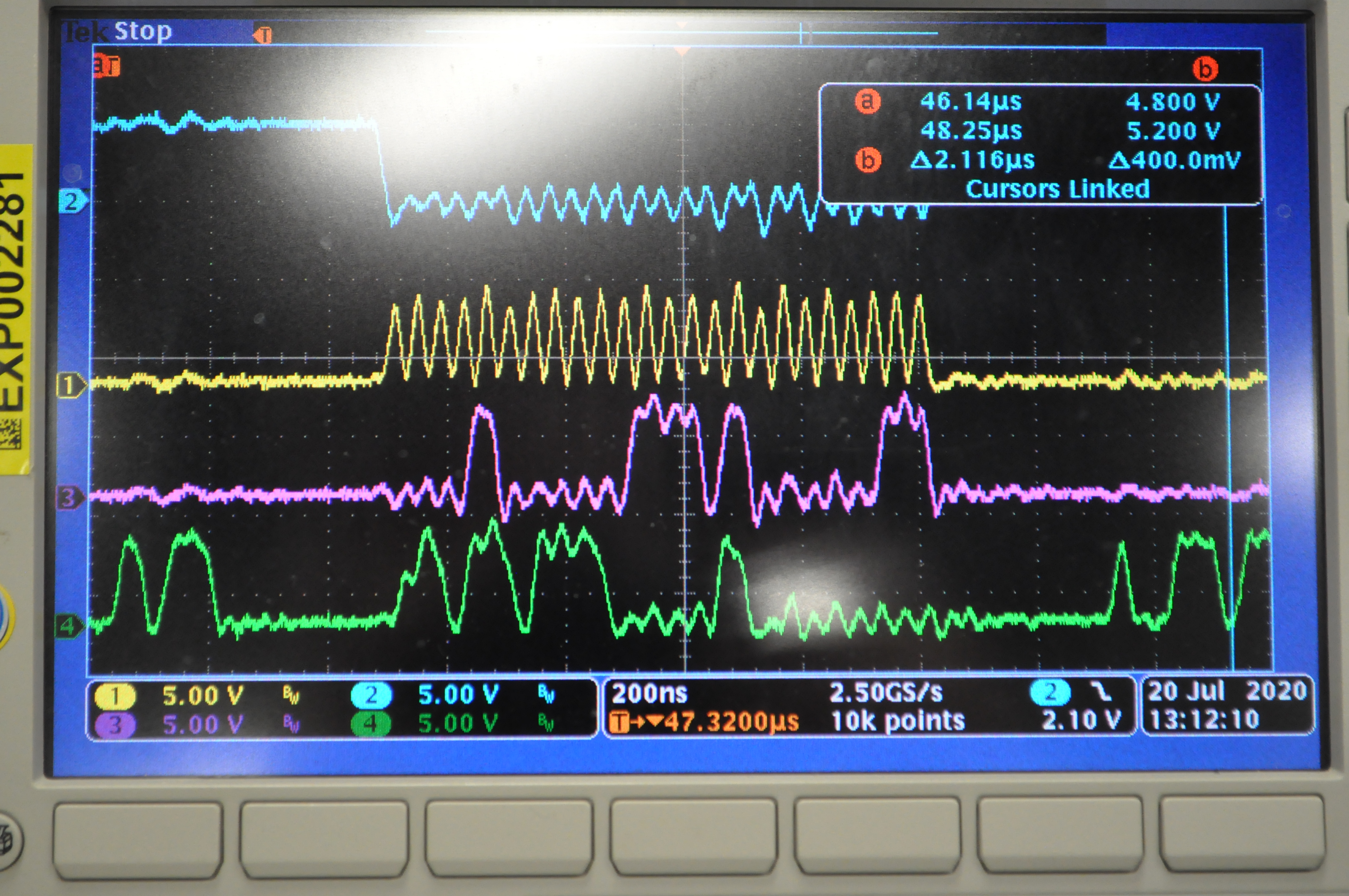
I am running the device in SPI-00.

Strangely, I am able to run the devices in manual mode and get all channels by sending writes to the channel ID register with 24-bit transactions of 0x08_1D_0X (X from 0 to 7), but would like to run in auto sequence mode in order to keep the SCLK Freq lower and still maintain max throughput. 

  • Hi Sean,

    Welcome to the TI E2E Community!

    Can you provide either a scope or logic analyzer capture of the SPI signals for the WRITE command?  /CS, SCLK, SDI, and SDO, similar to Figure 58 in the datasheet.

    Also, for the READ command, provide two 24b frames of data (two /CS cycles) (Figure 57) since the 8b register data is output on SDO on the following frame after the read command frame.

    Regards,
    Keith Nicholas
    Precision ADC Applications

  • Hi Keith, 

    Here is a capture of the data from all 6 ADCs simultanesouly

    The transactions are:

        --  WRITE DEVICE_CFG Addr = 0x1C Data = 0x02
        --  0x08_1C_02
        --  READ DEVICE_CFG Addr = 0x1C Data = 0x00
        --  0x10_1C_00
        --  WRITE AUTO SEQ CFG1 Addr = 0x80 Data = 0xFF
        --  0x08_80_FF
        --  READ AUTO SEQ CFG1 Addr = 0x80 Data = 0x00
        --  0x10_80_00
        --  WRITE AUTO SEQ CFG2 Addr = 0x82 Data = 0x01
        --  0x08_82_01
        --  READ AUTO SEQ CFG2 Addr = 0x82 Data = 0x00
        --  0x10_82_00
        --  WRITE SEQ_START Addr = 0x1E Data = 0x01
        --  0x08_1E_01

    The data received from the read to 0x1C is 0x00 (Should be 0x02)

    The data received from the read to 0x80 is 0xFF (Default Value) 

    The data received from the read to 0x82 is 0x00 (Should be 0x01)

  • Hi Sean,

    Thank you for the additional data.  Could you provide a zoomed up version for the first write and read command on one of the ADC's?  I want to check to see if there are any timing requirements that are not being met.  Please try to duplicate the waveform examples in Figure 57 and Figure 58.

    Also, please confirm the frequency of SCLK as well.

    Thank you,

    Keith

  • Hi Keith,

    This is from another run, so there's an extra transaction of all 0 after the read, but the behavior is identical

    --Write (0x08_1C02)

    --Read (0x10_1C00)

    --Finish Read (0x00_0000) All 0s received 

    SCLK is running at 25 MHz, this data is be captured with Vivado Chipscope at 250MHz 

    Thanks,

    Sean

  • Hi Sean,

    I do not see anything wrong with the waveforms that you provided.

    Can you confirm and measure the voltage on DVDD?  Double check the voltages on AVDD and DECAP as well.

    Also, please confirm that the IO voltages are at the correct level.  If possible, an oscilloscope capture of /CS, SCLK, SDI, SDO for one of the ADC's may reveal what is going on.

    If you are comfortable sharing a screen capture of the schematic for the ADS8168 section, showing the pin connections, I will double check.

    Regards,
    Keith

  • Hi Keith,

    I am not working on site today, so I can't provide any screen captures or exact measurements, but I did measure AVDD, DVDD, and DECAP and they were at the correct range and I also measured the IO, we have a level shifter taking 1.8V IO and shifting up to 5.0V and at the slower speed the level shifter is able to handle the data throughput

    AVDD: ~5.0V

    DVDD: ~5.0V

    DECAP: ~2.85V 

    What's very confusing is that register writes to register 0x1D from 0 to 7 (for all of the channels) (24-bit 0x08_1D0X) (x from 0 to 7) in a loop yields the expected data out for manual mode (and the digitized data is in line with what we are measuring on the AINs with internal vref of 4.096V), so clearly the devices are accepting the commands, as the read requests also show, but for some reason are ignoring writes to any other registers. 

    We initially had some pins not connected that are now jumpered and giving us the expected digitization performance, so we don't have an accurate schematic to share as of yet. 

    Thanks,

    Sean

  • Any further assistance? We are still stuck not able to perform other writes to other registers

    Thanks,

    Sean 

  • Hi Sean,

    I am out of ideas, unless you have some kind of signal integrity issue that does not show up in the logic analyzer measurements.

    I have asked one of my colleagues to also take a look at this to see if he has any additional ideas.  I will provide an update to you once he has had a chance to look at this.

    Regards,
    Keith

  • Hi Sean,

    The team has looked at this, and based on the data you have provided, everything looks correct.  

    Again, best guess is that this is some kind of signal integrity issue that is not showing up in the logic analyzer measurements.  If possible, please provide a scope capture of the key waveforms for one of the ADS8168.

    Regards,
    Keith

  • Hi Keith,

    My initial solution was able to meet the application initially, but we are continuing development with this board and would like to be able to interface with it.

    I was able to hook up a scope and have been noticing some unusual behavior. I'm not able to get a scope capture yet, but should be able to get one tomorrow. 

    I'm noticing that the MISO from the ADC is active when the chip select line is high and no clock is being provided? 

    This behavior comes after I increased the delay between transaction from ~32 cycles of delay to ~128 cycles. 

    Do you know what could cause this kind of behavior? 

    Thanks,

    Sean 

  • Hi Sean,

    SDO-0 line (MISO) goes high-z when chip select is high.  With the increased delay, it is possible you have leakage currents that are pulling this line high, and it is not actually being driven high.  You can add a 1kohm pull-down resistor between MISO and GND, and if this is the case, the line should stay low.  If not, then something in the system is driving the line high.

    Do you have any other devices connected to the MISO line, other than the ADS8168 and the processor?

    Regards,
    Keith

  • Hi Keith,

    I'm still working on the scope traces.

    It doesn't look like the line is pulling temporarily high, it looks more like a full data transfer, multiple times, where the line is clocking out data, and no longer synchronizes with the chip select or input clock. The data is coming regularly at about ~400kHz rate while the chip select is off. Anytime I then proceed to attempt a transaction, the chip output is near garbage. 

    We have a SN74LVCH16T245DL level shifter in line, nothing else between an FPGA and the ads8168. 

    Thanks,

    Sean

  • Hi Keith,

    Finally got some pictures of the Scope

    Top is Chip select

    2nd is clock

    3rd is mosi

    4th is miso

    The first one is nominal running the initial sequence, After the level shifter from 1.8V I/O to 5V I/O 

    The Second one is zoomed in

    The third one is after changing the delay

    The fourth and all following are zoomed in after changing the delay

  • Hi Keith,

    As a follow up to my responses yesterday, we pulled the MISO signal from the ADC off of the level shifter and the signal immediately cleaned up and stopped sending anything in the middle of the chip being inactive. 

    It also stopped reaching ~1/2 range of the 5V as seen in the pictures from before. 

    We attempted to add on a pull down and a series resistance between the ADC and the level shifter but that has not fixed the problem. 

    We are using the SN74LVCH16T245DL from B -> A shifting down from 5V to 1.8V both the output enable pins and directions pins are grounded. 

    We are using the same part from B->A to shift up from 1.8V to 5V with no issue on that side similarly the enable pins and direction pins are grounded as well. 

    Thanks,

    Sean 

  • Hi Sean,

    This looks like some kind of bus contention issue, where both the ADS8168 and another device are driving the MISO line at the same time.  You mentioned removing the ADC cleaned up the signal.  Can you probe the MISO line at the FPGA side to see if there is any activity on this pin? 

    Also, with the SDO line removed (connected to nothing on your board), directly probe the pin to see if there is any activity on it when /CS is high.

    The ADS8168 should never drive the SDO line (MISO) with chip select high.  If it is determined that it is driving the line, then it is damaged.

    At this point, It could be a damaged ADS8168, or a damaged/miswired SN74LVCH16T245DL, or possibly an incorrect configuration in the FPGA itself.

    If you would like to share a screen shot of your schematic, showing the connections between the ADS8168, SN74LVCH16T245DL, and the FPGA, I would be happy to look it over.

    Regards,
    Keith

  • Hi Keith,

    It ended up being the SN74LVCH16T245DL.

    It was damaged, when we replaced it, the bus worked as expected! 

    Auto-sequencing mode also worked as expected now. 

    Thanks so much for looking at this for us.

    -Sean 

  • Hello Sean,

    This is great news!  Thanks for sharing the update.

    Regards,
    Keith