This thread has been locked.

If you have a related question, please click the "Ask a related question" button in the top right corner. The newly created question will be automatically linked to this question.

ADS127L01: No output from adc

Part Number: ADS127L01

Hi,
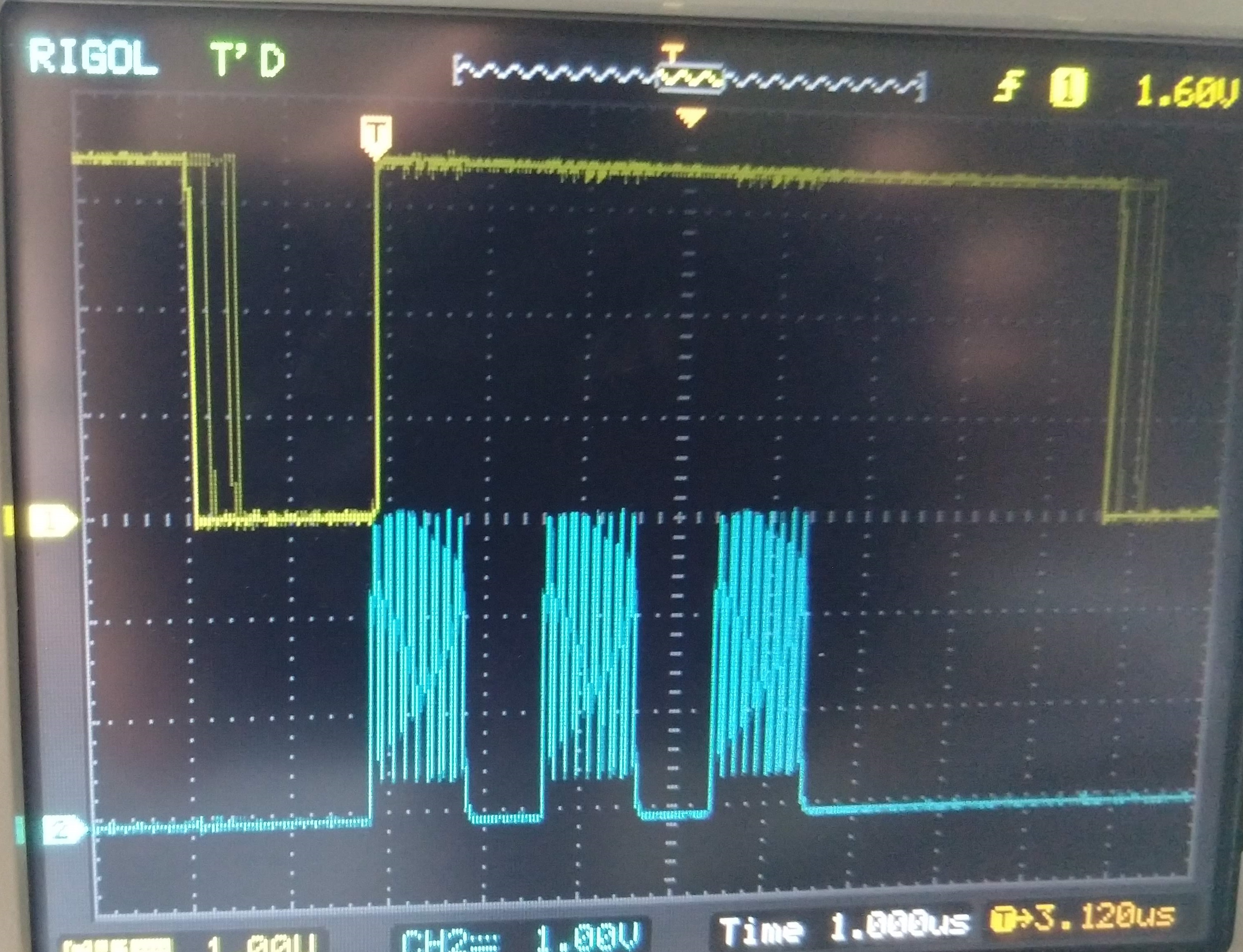
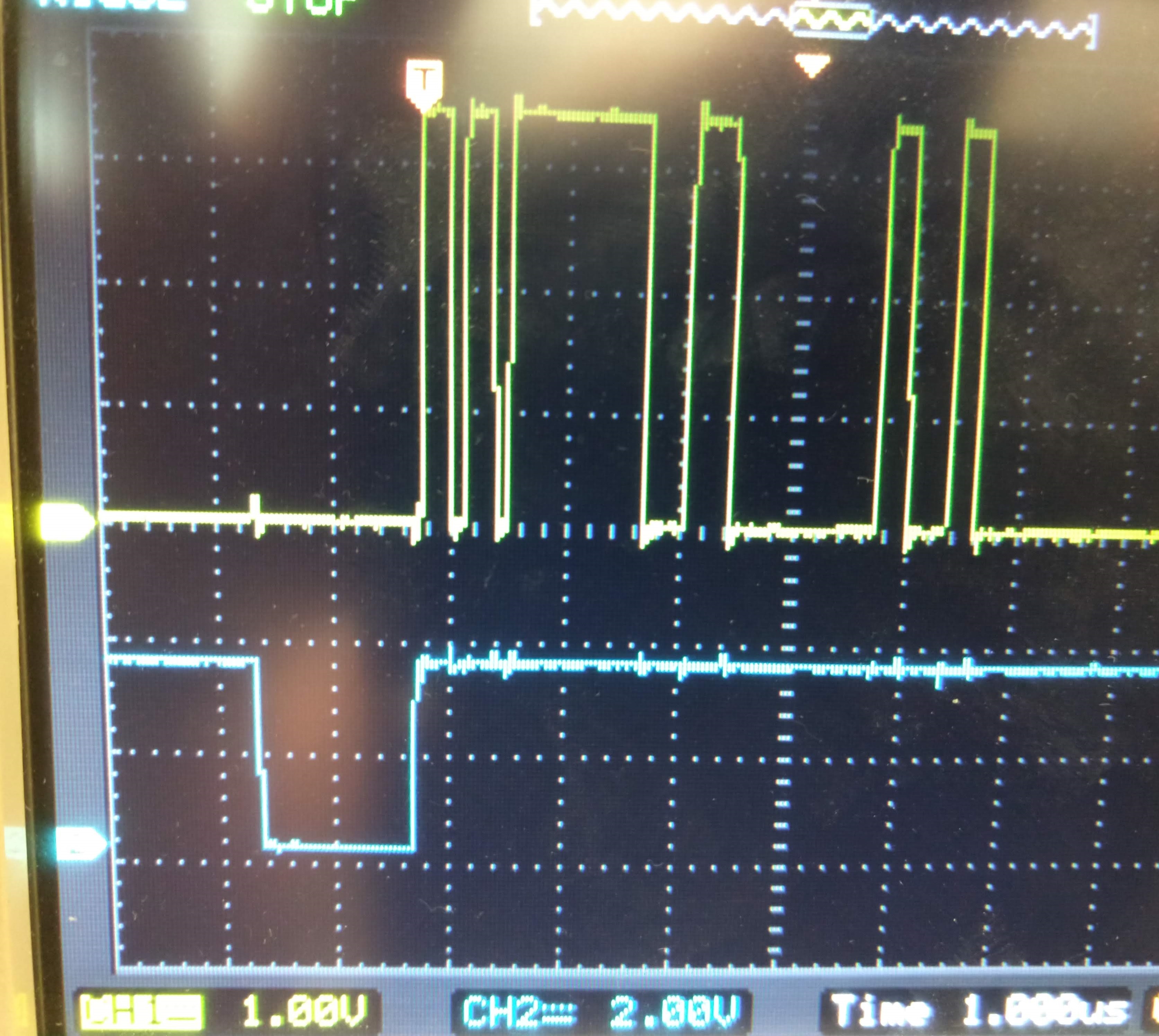
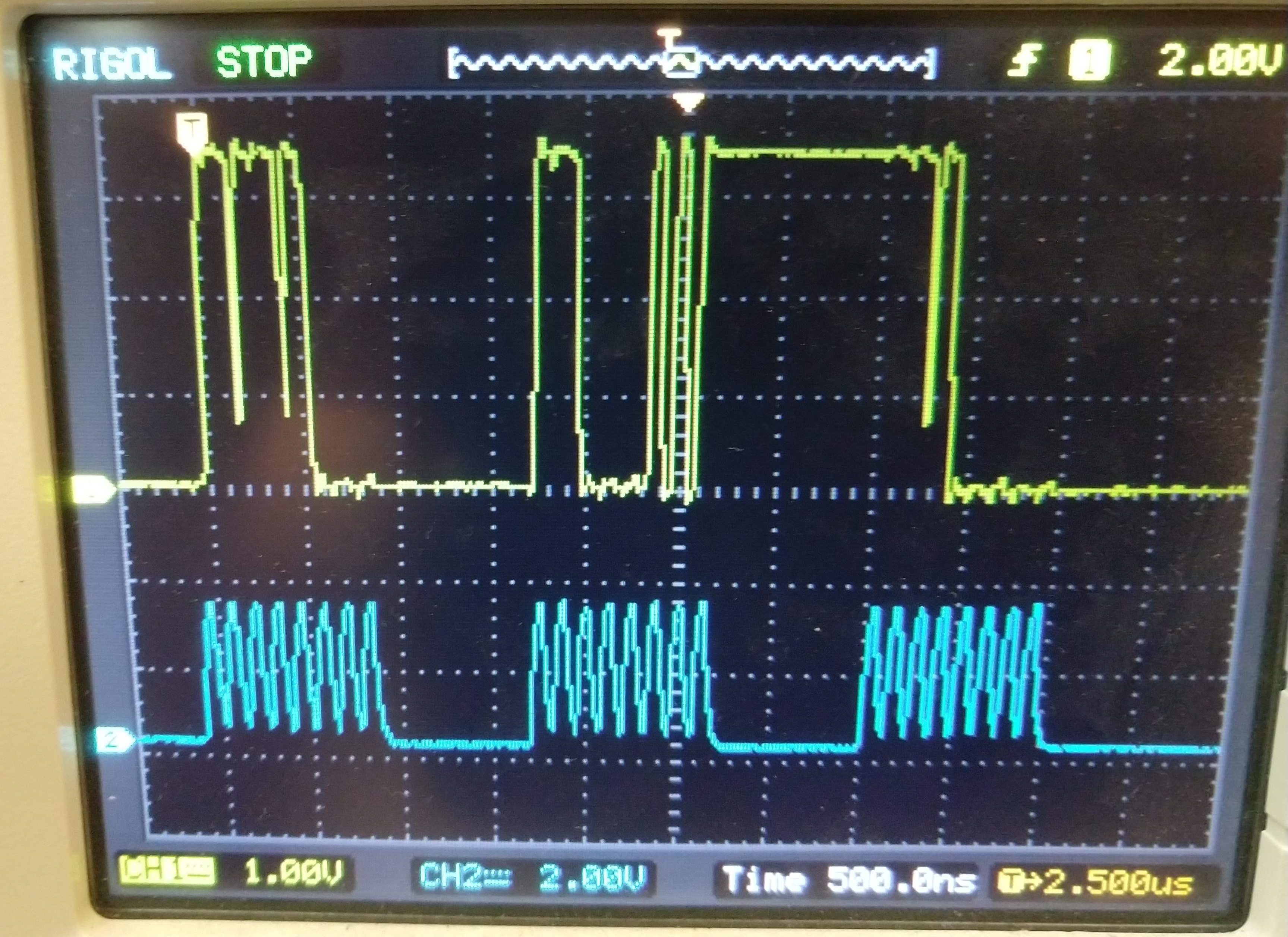
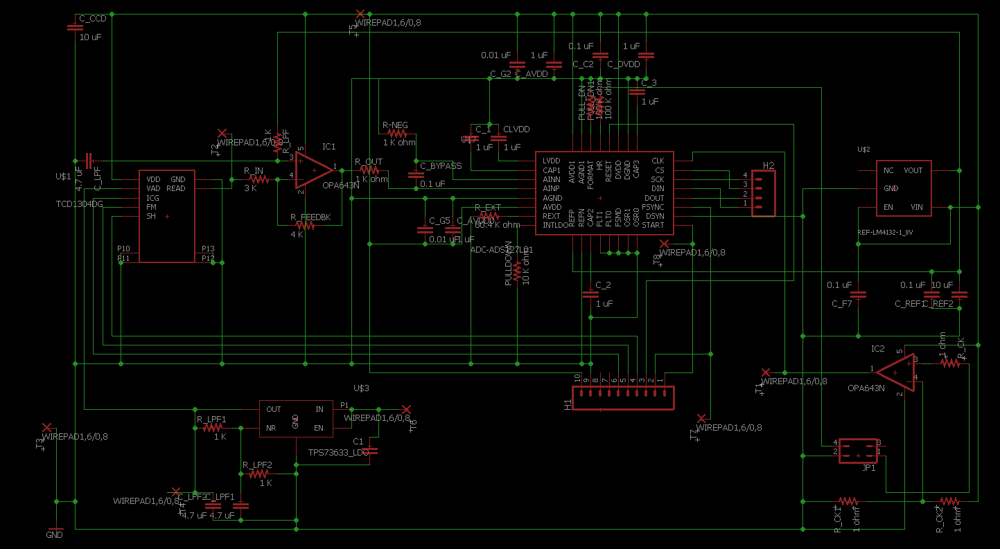
I am not getting readings from my ADS127LO1 adc.  My scope shows the clock cycling at 8 MHz. The DRDY pin spends most of the time high and toggles low for about 2 us.  The DRDY cycle period is 8 us.  I have my microcontroller set to read three bytes of data after the falling transition of the DRDY pin. My scope shows three sets of pulses (8 pulses per set) from the SCK pin.  My microcontroller is not registering any data recieved, and my scope does not show any pulses coming out of the DOUT pin. Disconnecting the wire from the DOUT pin to the microcontroller does not help.  My familiarity with SPI is rather limited so I don't know if this software or hardware related.  Any help is appreciated.  Some info on connectivity is below.

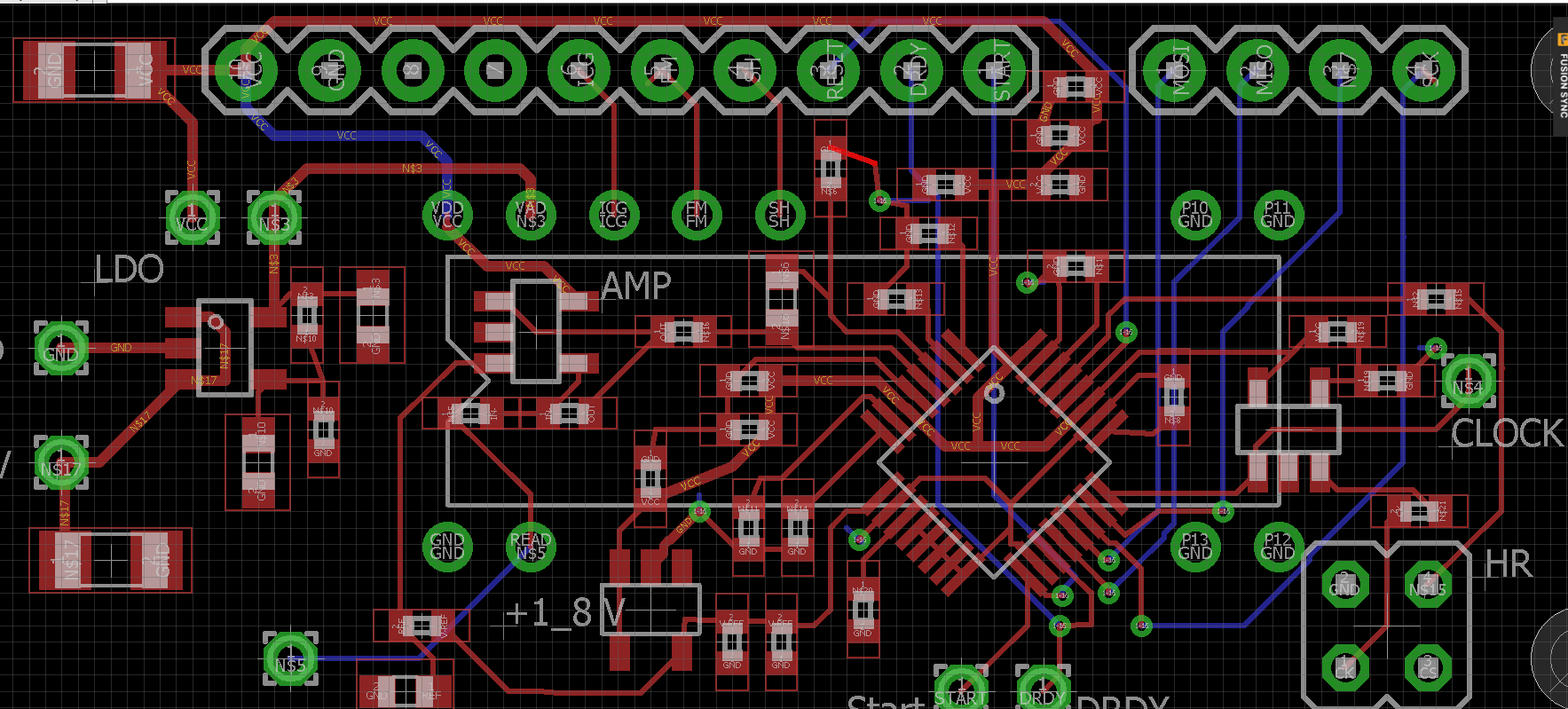
My DVDD and AVDD are tied together at 3.29 volts. All my grounds are tied together. I have RESET and START pulled high and the following pulled low: CS, DSYN, DSYN, FLT0, FLT1, FSMD, OSR1, OSR0, INTLDO, FORMAT and HR.   According to my multimeter, my input to the AINP pin is about 1.5 volts, AINN is pulled to ground.

Thanks,

Jack

  • Hi Jack,

    Thank you for choosing the ADS127L01 device.  While you've provided a good description, would it be possible for you to share a screenshot of the SPI timing signals going into the ADS127L01 device?  It really helps us debug these situations.  The device sounds like it's cycling /DRDY waiting for you to pull data from the data buffer.

  • Hi Collin,

    Thanks for getting back to me so quickly. 

    The two pics below show the scope traces with the DRDY pin and either the CS or MISO pin.  The MISO pin is not cycling, the CS pin is.  The MOSI pin is doing nothing, just like the MISO pin.  If the ADC is waiting for a signal from me, then that is what the problem is.  If so, please point me to a description of what it is expecting.

    Thanks again,

    Jack

  • Today I got more information on this issue.  It looks like I can get data for a short period after resetting the ADC:

    Today I wired the reset pin to a 20 Kohm pull-up resistor connected to vcc.  When I touch a ground wire to the circuit, a get transient output on the MISO pin.  By transient, I mean that it stops outputting data after a while. I have seen it stop after sending as few as 9 three byte values and I have also seen it continue outputting data for >10 second.  The attachments below show one-shot scope traces triggered off of MISO on channel 1 (yellow).  The first trace shows DRDY on channel 2 (blue), showing that the MISO output is timed to the DRDY pulse.  The second trace shows the SCK on channel 2. 

    Any suggestions on what could be going wrong?  I will be happy to hear of other tests that could help with diagnosis.

    Thanks,

    Jack

  • Hi Jack,

    You stated that your CLK input is a continuous 8MHz.  Also, you have the part configured for LP mode which does support an 8MHz clock.  Can you confirm that you have a 60.4kOhm resistor connect to the REXT pin to AGND to support LP mode?

    Also, with your filter setting (Wideband 1), and OSR setting (32), you should get a conversion rate of CLK/OSR=8M/32=250ksps, or 4uS data period.  This is the frequency that DRDY should also toggle.

    Since the data rate is 250ksps, or 4uS, you need to clock the data faster than this rate, or you will get corrupted data.  From the above scope waveforms, you are taking more than 6uS to clock the data out.

    I suggest trying the following:

    Set your main clock input (CLK) to a much lower frequency, for example 1MHz.  With the MOSI pin set to GND (DIN), and no SCLK, you should see the DRDY line toggle at 1M/32=31.25ksps, or every 32uS.  The high time for DRDY in this case should be 2 CLK periods, or 2uS using a 1MHz CLK.  Once you confirm this, then try reading data from the ADC by sending 24 SCLK pulses.

    If you still get corrupted data, we may need to look at your board layout.

    Regards,
    Keith Nicholas
    Precision ADC Applications

  • Hi Keith,

    Thanks for your help.
    It looks like I provided a piece of incorrect information (Sorry about that).  The main clock is not running at 8 MHz as I had said.  The scope trace shows the clock pin running at 3.3 MHz.  It appears that I changed it while troubleshooting and it never got changed back. Given that I am inputing a 3.3 MHz clock, I think I should expect a 9.6 us DRDY period, which is what I see on the scope.  Given this value, I think the SCK frequency should be acceptable, should it not?  To check, I doubled the SCK frequency to fit within 4 us.  That had no effect.
    Adjusting the clock to 1 MHz gives 1 us clock time, 32 us DRDY period. Grounding MOSI and SCK, the DRDY pulse is high for 4 us (not 2 us as you say it should, is this a problem?).
    Regarding the resistor value on the REXT pin, my multlimeter reads 60.7 kohm.  I read 1.205 volts on that pin.

    I will upload board info as soon as I get out of a meeting that I  am late for.

    Thanks again,

    Jack

  • Eagle board and schematic screenshots.  The circuit is intended to read a linear CCD array (bottom face of the board). Signal from the CCD is inverted and amplified by the AMP on the upper left.  Analog input to the CCD is from an LDO in upper left.  Ten pin header carries signal to the CCD and also the RESET, DRDY, and START pins.  Four by one header carries SPI signals.  Two by two header in lower right carries clock for ADC and HR pin.  LDO and CCD are not populated while I am prototyping the ADC.  Right now, I am inputting voltage to the ADC from the wiper of a pot with the other pins tied to VCC and GND.  The circuit board will connect to another circuit board that contains a TM4C123 microcontroller.  While troubleshooting this issue, I am using a Tiva LaunchPad, a breadboard and jumper wires instead of my custom microntroller board.

  • Hello Jack,

    Based on a CLK frequency of 3.3MHz, you should be meeting all timing requirements.  However, for initial debug of code and hardware, I would suggest you keep the CLK at 1MHz to help with any signal integrity issues.  

    Regarding the minimum DRDY high when not reading data, this is probably a misprint in the datasheet; 4uS does not indicate a problem and the frequency of DRDY is correct based on your 3.3MHz CLK frequency.

    Also, you do seem to get data for a short period of time, but as you had stated, the board is sensitive to noise and will stop communicating.  This is either due to noise getting into the START, RESET, or one of the mode control pins.  It could also be due to noise on the power supply lines, causing an internal power-on reset.  The placement of the supply bypass capacitors is very important for proper operation, as well as the ground connections to these capacitors, which should be tied into a solid ground plane directly beneath the top side components.  Many of your supply capacitors are not in an ideal location, and this could make the part susceptible to random resets.

    Figure 131 in the datasheet shows an example board layout, and should be copied for best performance.

    At this point, I think this is likely layout related, and I am not sure how to make it more robust on your existing layout.  For development, I suggest you get an ADS127L01EVM.  You can connect your own MCU hardware to this board and use it to get communications working.  The EVM also includes a good reference and input buffer circuit that you can tie into the rest of your system.  Once you get everything working with the EVM, you can then use the EVM as a reference design for a custom board layout.

    Regards,
    Keith

  • Hi Keith,

    I think you are absolutely correct about the issue being related to noise on the board.   The CCD has a clock that runs at 1 MHz. I just disconnected the wire that runs the CCD clock and now the ADC MOSI output looks the way you would expect.  I will mark this thread as solved since I feel that I now have the tools I need to get the problem solved.  Thanks for pointing me toward the evm.  I do not think I will buy one, but having the design information from the user guide should help.

    Best,

    Jack