This thread has been locked.

If you have a related question, please click the "Ask a related question" button in the top right corner. The newly created question will be automatically linked to this question.

ADS1263: jump points

Part Number: ADS1263

Hi sir,

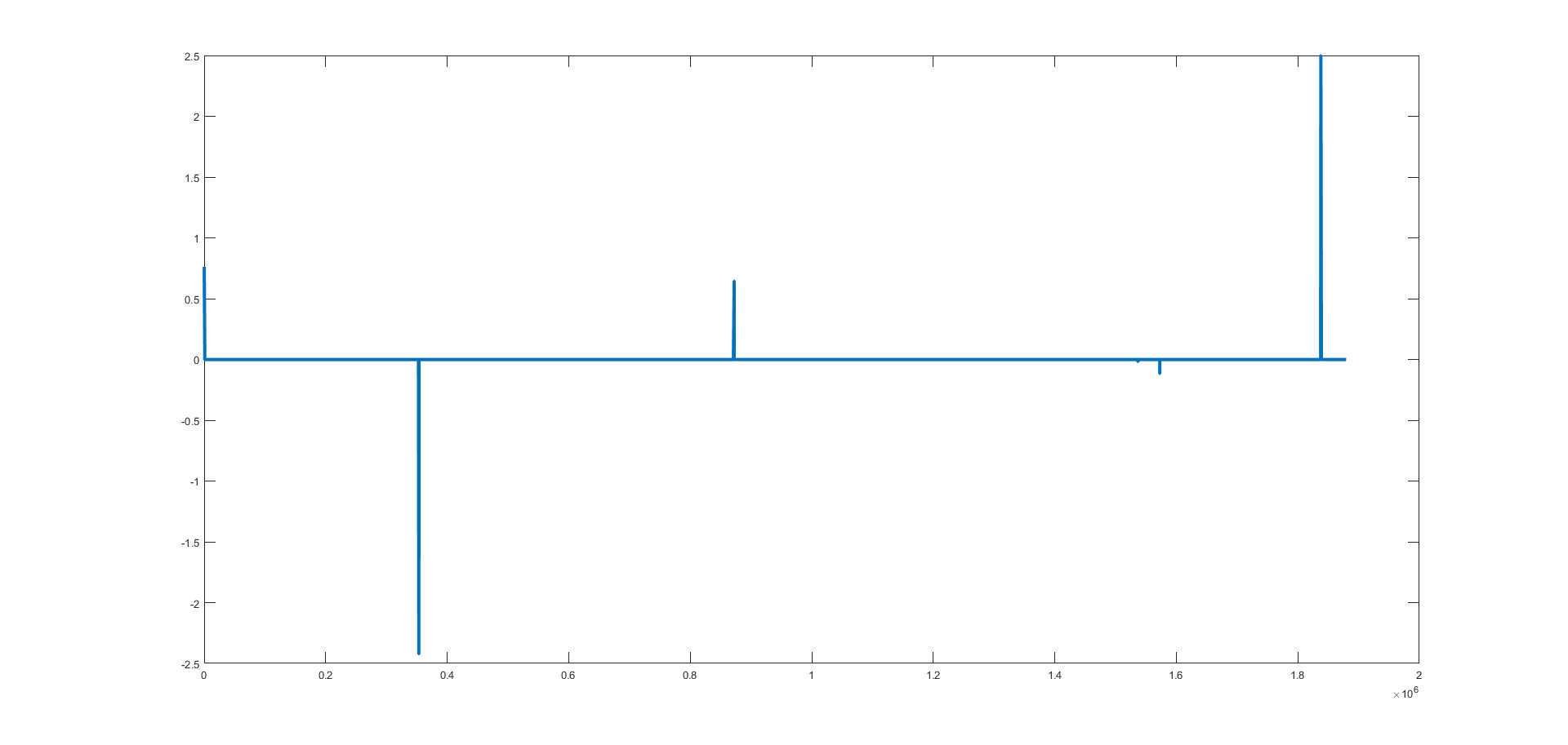
  There are some jump points when data convering. I have changed the data rate from 20sps,100sps, 400sps and filter types, but the issue still exist. The jump point is only one sample point at any time. The following figure is 400sps, sinc4 filter. and GND input.

  Please help me, i have no idea anyway. Thank you and godness.

  • Hi user3677382,

    Can you please provide more information including how you did the test, your connection and schematic? thanks.

    Best regards,

    Dale

  • Hi Dale,

          Here is the sch. I use FPGA to read the ADC data. The procedure is like this:

          1) power on,delay 1.3S

          2)send STOP2 command,delay 1.3S

         3) set Start High

         4)If (Drdy==0) ,read the data from  DoutDrdy

         5) send the data to PC by COM port

      And, I also check the Serial Interface by Oscilloscope, the FPGA timing is OK. However, there is  an abnormal state. The  value of the status Byte usually is 41h. Sometimes, the value is 7FH,5FH, and the jump points comes out. 

      If I clear the reset bit at step 2), the normal status Byte is 40h. And it also will jump to 7FH or 5FH at one sample point, then change back to 40h.

  • Hi Dale,

          And there is another experiment. I set the (06h)==CCh or (06h)==DDh, the jump points still comes out.

  • Hi Dale,

          Update.

          The Refout pin is 0V. Is it right?

  • Hi user3677382,

    I did not see any issue from your schematic only except you need a 0.1uF decoupling capacitor between the power supply A+2.5V and A-2.5V.

    By default, the internal reference is already selected for ADC1 after the device is powered up:  the INTREF bit in POWER register is "1"  to enable internal reference, also the RMUXP[2:0] and RMUXN[2:0] are "000" to select internal reference for ADC1.

    When the ADC is powered with a single +5V supply, the voltage shown on REFOUT pin will be +2.5V which is the middle voltage of (AVDD-AVSS). When the ADC is powered with dual +/-2.5V supplies, the voltage shown on REFOUT will still be the middle voltage of (AVDD-AVSS) which is 0V in your design. Hence, the voltage you measured on the REFOUT is correct.

    Also, you mentioned that "I set the (06h)==CCh or (06h)==DDh, the jump points still comes out." the result you observed is correct, the "CCh" written to the INPMUX (06h address) register selected analog power supply as ADC's input,  the "DDh" written to the INPMUX (06h address) register selected analog digital supply(+3.3V) as ADC's input, thus both supply voltages to ADC's input are equal to or higher than the maximum input range (FSR) of the ADC, so the output conversion will definitely reach the maximum value which was the jump point you observed.

    I do not know whether the signal you applied to AIN0 came from a precision and stable signal source or not when you did the experiment without programming the INPMUX register. However I suggest to apply a stable and clean voltage signal to AIN0 input, for instance 1V, then check the output code from the ADC. Also, a RC filter on input channel will be very helpful to filter any noise to the ADC.

    Another way you can do the test is using internal TDAC to create a proper test voltage as the ADC1's input for ADC self-testing and verification, please see the section 9.3.12 Test DAC (TDAC) for the details.

    Best regards,

    Dale

  • Hi Dale,

           Many thanks for you response!

           I just connected AIN0 to GND directly when I did all the test. 

           If I remove the 1uF captitor on the REFOUT and AVSS, the output have a very big noise.such as 0.1V P-P value. I suposed maybe the REFOUT is the key point. I also did the TDAC loopback test, the jump point sitll exist. Would you please help me to send the layout of the TI demoboard?


  • Hi Dale,

          Could you please help me why the STATUS BYTE jump to 7FH or 5FH?

  • Hi user3677382,

    The capacitor on the REFIN/OUT pin is very important when we design any ADC circuit, this capacitor will filter the noise from the internal reference circuit. Also, this capacitor should be placed to the ADC device as close as possible on your board. I'm trying to find the layout however I do not have it right now. The capacitor (C10) on the REFOUT pin on the EVM board is shown on the location below in the following picture from the ADS1263EVM User's Guide.

    When you talked about the jump value of the status Byte, do you mean the jump point is only showing up in the "status" location in the following picture for Read Data Direct mode? Can you provide the entire timings in a frame?

    Best regards,

    Dale

  • Hi Dale,

         The timing on the Status Byte is as followiing.the yellow channel is SCLK, and the green channel is Data

  • Hi Dale,

          In fact, there are four ADS1263 on one PCB board. And I find if make only one ADS1263  active, it can work well. Howere, two ADS1263 CAN NOT WORK TOGETHER. Maybe ADS1263 is very weak to cross-talk on the power supply. Here is my layout. Please help me to give me some advise, and i will do the next version asap. Many thanks!

  • Hi user3677382,

    It's very hard to address the issue from your limited information. 

    1. Is the device showing jump points in a specific device or channel location on the board?
    2. Is the jump point only shown in "status" position in the timing graph I showed to you?
    3. Is your picture showing a good timing without a jump point? if yes, can you please show me a timing with jump point also for all digital signals including SDI and /CS?
    4. Is the GND in Layer2 same as the GND on the bottom Layer and shorted together? If yes,  you design a singe point connection for each ADC to the GND on the board, are you designing this layout for using a shield for each ADC on top layer?

    Looks like these four ADCs are using completely different interface to the FPGA, please confirm. A whole schematic including power supplies will be helpful.

    Thanks&regards,

    Dale

  • Hi Dale,

    1. Is the device showing jump points in a specific device or channel location on the board?
    2. [comments]:all the channel and device show the same symptom. Single channel works well, over two chanels will come out jump points. 
    3. Is the jump point only shown in "status" position in the timing graph I showed to you?
    4. [comments]: Yes. The "status" byte abnormal must come with the jump points. However, the jump points will come out while the "status" is ok, sometimes. 
    5. Is your picture showing a good timing without a jump point? if yes, can you please show me a timing with jump point also for all digital signals including SDI and /CS?
    6. [comments]: Sorry, the picture is not the right one. /cs, din are low.
    7. Is the GND in Layer2 same as the GND on the bottom Layer and shorted together? If yes,  you design a singe point connection for each ADC to the GND on the board, are you designing this layout for using a shield for each ADC on top layer?
    8. [comments]: Yes. I can not fully understand how to do "you design a singe point connection for each ADC to the GND on the board". the rectangle on the top layer is for shields for each ADC. And i have shield them for a test, the symptom is the same.

    Looks like these four ADCs are using completely different interface to the FPGA, please confirm. A whole schematic including power supplies will be helpful.

    [comments]: the four ADCs interface come out from different pins of FPGA, but the timing is completely same in the FPGA, the timing different should be in ns level. 

  • Hi Dale,

         Could you pls help me to forward this message to TI ADC layout specialist, and give me some advices about how to do about these 4 ADS power suplly and layout?

  • Hi user3677382,

    Apologized for the late response. I'm helping you to address the issue.

    For your answer in 5 above, I'm trying to understand how "the status byte abnormal must come with the jump points", also I'm thinking why only status bits are affected on the DOUT line. I guess the status byte is configured and desired by you, however the first picture in your post did not show the status byte. Also, the scope timing did not help without more information. What I really want to see is, the timing plots captured by a scope with jump points and status byte like the Figure 108 or Figure 109 in the datasheet, I want to see how the jump points are shown within the status byte on the DOUT output.

    The singe point connection means you are not using a solid ground for the board and you are connecting the ground of each ADC to the system ground through the notch of the shield case.

    Also, I would like to confirm with you if there is no any connection between the circuits of each ADC except the power supply and the ground. I did not get a whole schematic and layout database from you, thus need to confirm.

    Thanks.

    Best regards,

    Dale

  • Hi Dale,

         Maybe there is some misunderstanding about the "status byte". I mean, If the "status byte"==7F/4F, the data bytes after status byte is a jump point value. and if status byte==41(normal value), the data bytes maybe a jump point value.


         could you please give me your email? I will send the whole schematic and layout database for you. and the design tool is altium designer, is it OK?


  • Hi user3677382,

    We always use Altium and no problem, please request a friendship here to contact. Also, the timing plots captured by an oscilloscope including all digital signals will be helpful.

    Thanks&Best regards,

    Dale

  • Hi Dale,

        Done with the friendship requirement..

  • Communicating and checking the database offline.

    Best regards,

    Dale