Other Parts Discussed in Thread: ADS52J90, , ADS5294EVM
My original thread had been locked before I found a solution to my problem. See the post for the full background.
https://e2e.ti.com/support/data-converters/f/73/p/892927/3320071#3320071?jktype=e2e
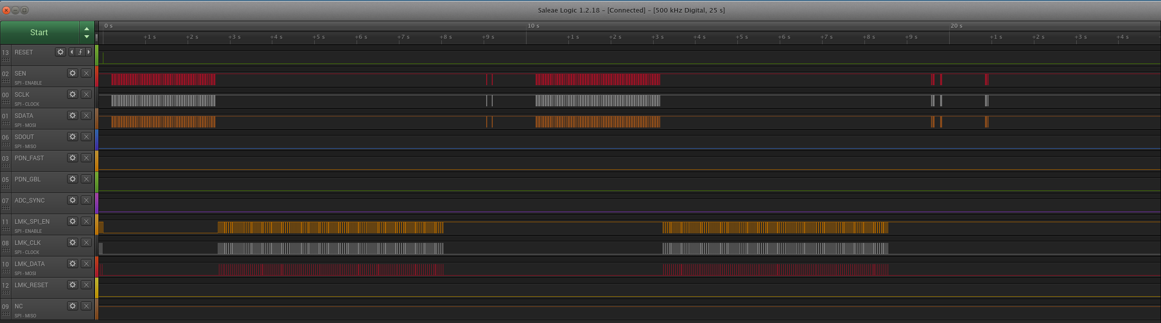
To summarize, I'm having trouble communicating with the ADS52J90 chip on the ADS52J90EVM board. I do NOT have the TI supported host FPGA cards (TSW14J56EVM or TSW1400) connected. Instead I'm connecting the ADS52J90EVM to a ZC706 board. I'm using the FTDI D2XX library and some C code to control the SPI bus in a bit bang mode. I'm fully aware that I will need to setup all the register settings in the ADC and clock distribution chip myself without the supported host boards. However, I can't get the ADC to read back any registers to confirm that my register writes are correct.
My test is the following.
1. Write address 0x00 = 0x0001 to reset the ADC chip
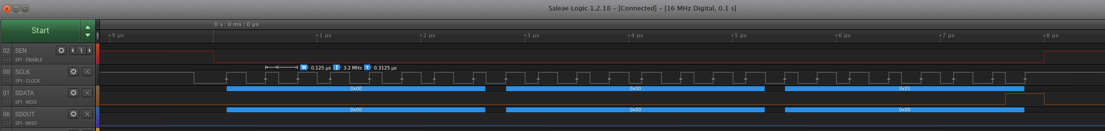
2. Write address 0x0A = 0x3000 to initialize the ADC chip. This step is specified in the ADS52J90 datasheet.
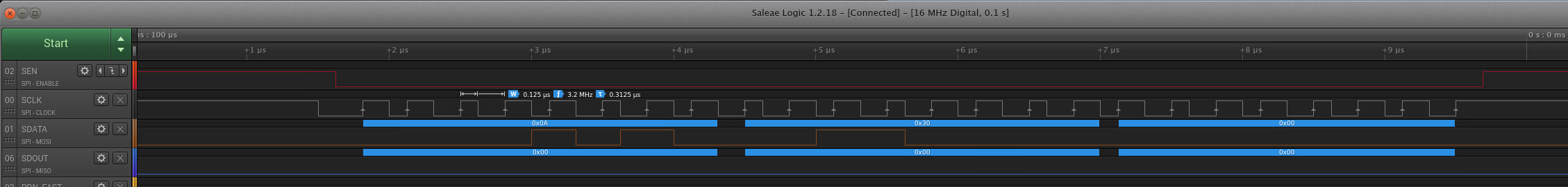
3. Write address 0x01 = 0x0094 as a test of the register writes. This should configure the ADC into 16 channel input mode.

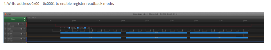
4. Write address 0x00 = 0x0001 to enable register readback mode.

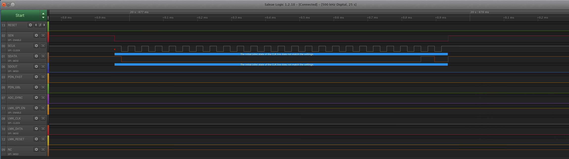
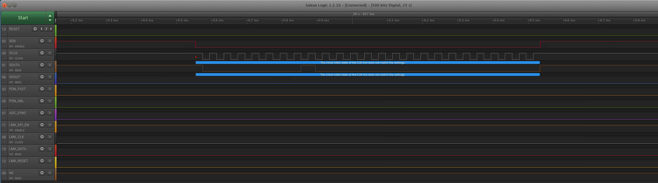
5. Read address 0x01.
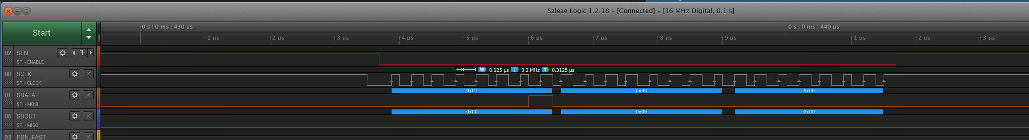
6. Read address 0x00.

The problem is that every read that I perform, I only see SDOUT (SPI-MISO) as 0. I have the SPI bus pins probed with a logic analyzer to confirm the transaction is according to the datasheet. I have even double checked that the logic analyzer is reading the SDOUT test point correctly by probing with an oscilloscope.
I suspected two things in my original thread that I have since tested.
1. Maybe the ADS52J90 requires a system clock for the registers to work properly.
I connected a signal generator with an 80 MHz clock output to J75 SMA input of the ADS52J90EVM. I reran my SPI test and got the same result. SDOUT always reads back 0.
2. Maybe the ADS52J90 has a minimum SCLK speed even though it is not listed in the datasheet.
My original test used a python script to bit bang the SPI transactions and it ran very slowly. SCLK was around a few kHz. I have since updated my test code to C and use the FTDI D2XX library. SCLK is now running around 3 MHz, which is less than the maximum of 20 MHz specified in the datasheet.
What am I missing? At this point, I'm starting to think the ADC is broken.
Thanks,
Chris