This thread has been locked.

If you have a related question, please click the "Ask a related question" button in the top right corner. The newly created question will be automatically linked to this question.

DAC38J84: SYSREF and DAC output timing variation etc.

Part Number: DAC38J84
Other Parts Discussed in Thread: LMK04828

Hi team,

This is a re-post to the DAC forum from the following URL.
In addition, the question has been updated.
e2e.ti.com/.../3409946

We are currently using a Xilinx FPGA Kintex-7 and a Xilinx JESD204 IP core to output analog signals with a TI DAC (DAC38J84).
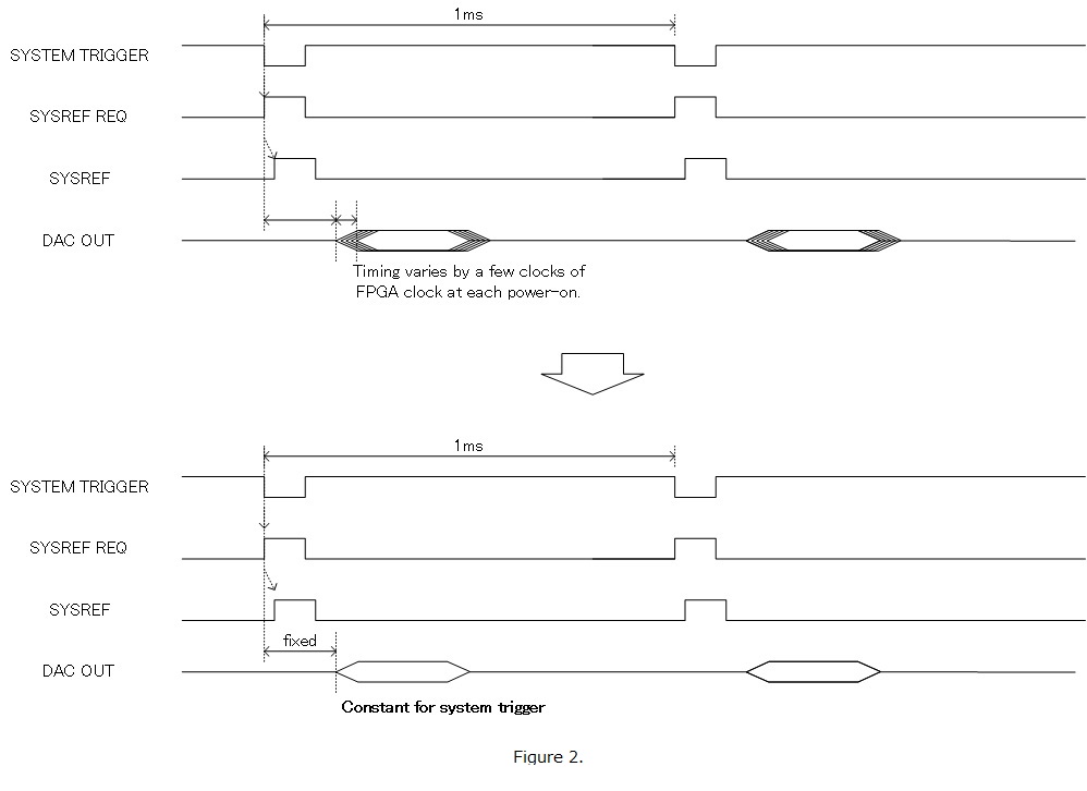
For example, the FPGA receives triggers every 1ms and needs to output an analog signal at that timing, but the analog output timing fluctuates between a few clocks in the FPGA clock every time the power supply is turned on.
However, the analog output timing varies between several clocks at each power supply startup, and we would like to output analog signals at the same timing.
We are using the JESD204B in Subclass 1, but since we do not have much experience with Subclass 1 and do not understand the operation of the JESD204B, we would like to ask you about the following

"Operating Conditions"
DAC is DAC38J84 and LMK04828 is used for clock and SYSREF generation. (Figure1)
The FPGA is a Xilinx Kintex-7 with a JESD204 Subclass1 IP core.

"Questions"
Q1) For example, if the register is fixed to a certain setting, is the internal delay in the DAC constant or does it fluctuate?
For example, is the internal delay in the DAC for a certain register setting constant, or is there a factor that varies?
It may have something to do with the IP core of the FPGA, but I would like to know if it is possible to output analog signals without any fluctuation in the trigger timing at each startup.

Q2) SYSREF is generated by a system trigger and analog output is attempted. (FIgure2)
At power-on or resetting, the SYSREF timing and the analog output timing fluctuate.
(I can't be sure, but it appears to fluctuate between 1Multi-frame.)
I have referred to the following forums and others, but I haven't seen any changes.
Do you have any solutions?
Since the clock, SYSREF, and trigger are synchronized and do not show any variation, I think there is another problem.
e2e.ti.com/.../ f/73/p/793625/2940186?tisearch=e2e- sitesearch&keymatch=DAC38J84#2940186
Q3) I need to reset the NCO at every trigger timing by using SYSREF.
But if you look at the analog output, the phase changes every time.
If you look at the ringing seen at the time of reset, it changes in about 5ns period (192MHz?) in 1 Multi-frame, the SYSREF output timing and trigger period are fine.
Can you find out the cause of this problem?

Q4) "link configuration error" and "read_empty" flag. was written in the register.
Does this have something to do with the timing variation?
Currently, the connection is made by masking.
Also, what exactly is "link configuration error" and what does it mean?

We will send you the DAC setting information and register configuration file.

LMFS setting:4421

interpolation rate:8

RBD setting:31

K setting:32

NCO setting:32
0x3555_555555_555555 (DACAB path)
0x2000_0000_0000 (DACCD path)

dac38j84_config.xlsx


If you have any other points to note (settings, usage, etc.), I would appreciate it if you could give me some advice.


Best regards,

T.Karita

  • Hello Karita

    user6379132 said:
    "Questions"
    Q1) For example, if the register is fixed to a certain setting, is the internal delay in the DAC constant or does it fluctuate?
    For example, is the internal delay in the DAC for a certain register setting constant, or is there a factor that varies?
    It may have something to do with the IP core of the FPGA, but I would like to know if it is possible to output analog signals without any fluctuation in the trigger timing at each startup.

    Internal DAC JESD204 + DUC latency is deterministic by the design of the JESD204B subclass 1. For detail, you may refer to the following paper to describe optimizing RBD to ensure deterministic latency

    https://www.ti.com/tool/TIDA-00996

    user6379132 said:
    Q2) SYSREF is generated by a system trigger and analog output is attempted. (FIgure2)
    At power-on or resetting, the SYSREF timing and the analog output timing fluctuate.
    (I can't be sure, but it appears to fluctuate between 1Multi-frame.)
    I have referred to the following forums and others, but I haven't seen any changes.
    Do you have any solutions?
    Since the clock, SYSREF, and trigger are synchronized and do not show any variation, I think there is another problem.
    e2e.ti.com/.../ f/73/p/793625/2940186?tisearch=e2e- sitesearch&keymatch=DAC38J84#2940186

    This is also related to RBD adjustment. Please refer to the paper above for RBD optimization. 

    user6379132 said:
    Q3) I need to reset the NCO at every trigger timing by using SYSREF.
    But if you look at the analog output, the phase changes every time.
    If you look at the ringing seen at the time of reset, it changes in about 5ns period (192MHz?) in 1 Multi-frame, the SYSREF output timing and trigger period are fine.
    Can you find out the cause of this problem?

    Resetting NCO also reset NCO phase. To ensure continuous phase, the SYSREF frequency need to be aligned with NCO counter. Please see the following paper for detail:

    https://www.ti.com/lit/an/slaa696/slaa696.pdf?ts=1594849199821&ref_url=https%253A%252F%252Fwww.ti.com%252Fproduct%252FDAC38J84

    user6379132 said:
    Q4) "link configuration error" and "read_empty" flag. was written in the register.
    Does this have something to do with the timing variation?
    Currently, the connection is made by masking.
    Also, what exactly is "link configuration error" and what does it mean?

    Link configuration is the ILAS sequence check after the CGS stage. You will need to ensure the ILA sequence being send from FPGA matches the expected programmed ILAS. We typically ignore ILAS sequence as this does not really serve much purpose other than ID checking.

    Read empty means there is a SerDes rate mismatch between FPGA and DAC. Please double check if there are any rate differences or PLL not tracking each other issue. 8420.DAC3xJ8x ILA Sequence.xlsx