This thread has been locked.

If you have a related question, please click the "Ask a related question" button in the top right corner. The newly created question will be automatically linked to this question.

ADS54J64EVM: Device Clock and Sysref phase relation

Part Number: ADS54J64EVM
Other Parts Discussed in Thread: ADS54J64, LMK04828

Hello,


My customer is planning to connect ADS54J64EVM to their FPGA board via the FMC connector.

And as a practice, they tried to operate ADS54J64EVM itself without TSW14J56EVM or their FPGA board.

According to ADS54J64 Evaluation Module User’s Guide 2.3.1, they follow the following step #1 to #3.


1. Open the ADS54J64EVM GUI from the Start Menu All Programs Texas Instruments

ADS54J64 EVM.

2. After the GUI starts, verify that the green USB Status indicator in the top right corner of the GUI is

illuminated.

3. From the INTRO tab, press the Configure LMK04828 button labeled as "Fclk=983.04MHz".


After that, they observed DCLKOUT0(device clock) and SDCLKOUT1(sysref) by oscilloscope.

The phase relationship between them are different every power cycle.

They expected the fixed constant phase relationship between them because they are JESD device clock and sysref.

Why their phase relationship is not deterministic? What is wrong?

To get the deterministic phase relation between the, what does my customer have to do?


Best regards,


K.Hirano

  • Hirano,

    Not sure why this is. I have a feeling it has something to do with the register settings used by the LMK. Can you attach the LMK configuration file and send this to the high speed clock forum? They should be able to help with this issue.

    Regards,

    Jim  

  • Jim,


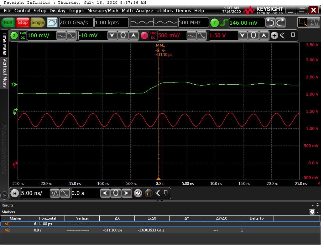
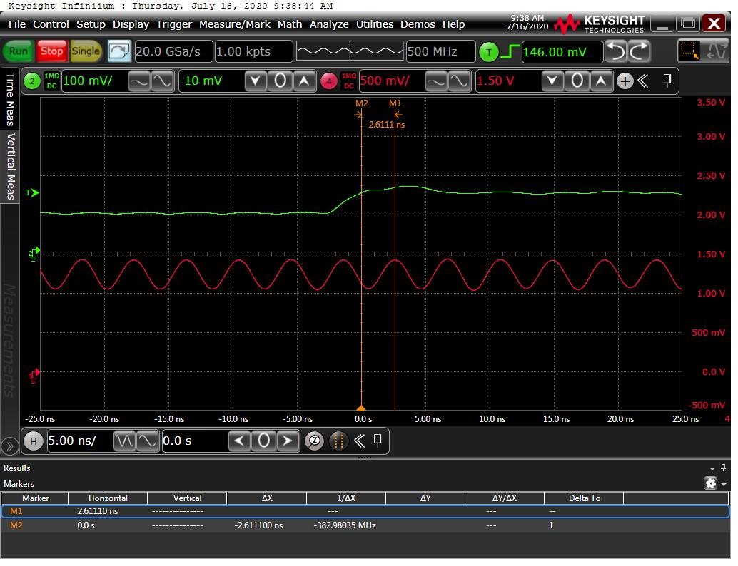
    I attach the two waveform plots, pattern1.jpg and pattern2.jpg.

    I also attach register damp, pattern1.cfg and pattern2.cfg respectively.


     /cfs-file/__key/communityserver-discussions-components-files/73/pattern1.cfg

    /cfs-file/__key/communityserver-discussions-components-files/73/pattern2.cfg

    Looking at two plots, there are 1/2 cycle of device clock phase differences between them.

    Please let me know what is wrong and how my customer can fix it.


    Best regards,


    K.Hirano

  • Hirano,

    Please replace the LMK04828_config2_983M.cfg file in the GUI configuration folder with the new one attached and give this a try. The location of this folder is shown in the attachment.

    Regards,

    Jim

    ADS54J64_LMK_Config.docxLMK04828_config2_983M.cfg

  • Jim,


    Thank you for providing corrected LMK04828_config2_983M.cfg file.


    My customer would like to know what were wrong and how they were corrected more detail to reflect those things to their design.

    Could you elaborate?


    Best regards,


    K.Hirano

  • Hirano,

    I had the LMK experts look at the two configuration files and they replied with the following message below. They also sent me an updated config file (attached). Four registers were slightly modified. These are the ones with comments added. If you have more questions regarding this, please post them on the high speed clock forum.

    Regards,

    Jim

    First, something’s weird with original LMK04828_config2_983M.cfg. The file says that OSCin frequency is 61.44MHz, and the OSCin clock is set as if for 61.44MHz, but the VCO divider is 24 with a prescaler of 2 (2949.12/(2*24) = 61.44MHz), and the PLL2 R-divider is set to 2 with the OSCin multiplier disabled (61.44MHz/2 = 30.72MHz), so the phase detector frequency doesn’t match. And if I assume that the VCXO frequency on OSCin is actually 122.88MHz, things make sense again (except the setting of 0x162 which is now incorrect, and could cause problems for the system with VCO calibration). The new file sets this correctly. I don’t think that causes the issue you see, but it’s something that needs to be addressed. I’m going to assume the VCXO frequency is 122.88MHz in all cases, in which case set 0x162[4:2] = 0x1.


    It makes sense to me that the files have a delay difference. The old file has the device clock digital delays set to CNTH=5, CNTL=5, and SYSREF set to bypass. The new file has digital delay disabled on all the clock outputs, CNTH=5, CNTL=5, and the SYSREFs are both set to bypass mode. Both files have the same SYSREF digital delay values. The digital delay values are going to be different by 10 VCO cycles, ± whatever the difference is for enabling digital delay in the first place. The customer measurement indicates about 2ns of difference, which at VCO=2949.12MHz corresponds to about 6VCO cycles of delay difference – I can’t totally account for the 10 vs 6 difference, but I suspect there’s a static offset between enabling/disabling digital delay on a divider.


    The easiest way to make the files behave the same is to turn on your digital delays (0x106 = 0x70, 0x10E = 0x70). Also, the new file should write 0x143 as 0x91 instead of 0x11 the first time, to ensure that SYSREF_CLR is set and the SYSREF digital delay counter gets reset when you power on the SYSREF_DDLY block.


    I saw a question in the new file comments, so to address that line: New file can write 0x140 0x01 in sync procedure, doesn’t look like you ever use the SYSREF pulser so power it down to save current. The SYSREF_PD and SYSREF_DDLY_PD blocks can (and for SYSREF_PD, must) stay on without disrupting operation.

    LMK04828_config2_983M_new_DPupdate.cfg