Hi team,
Good day.
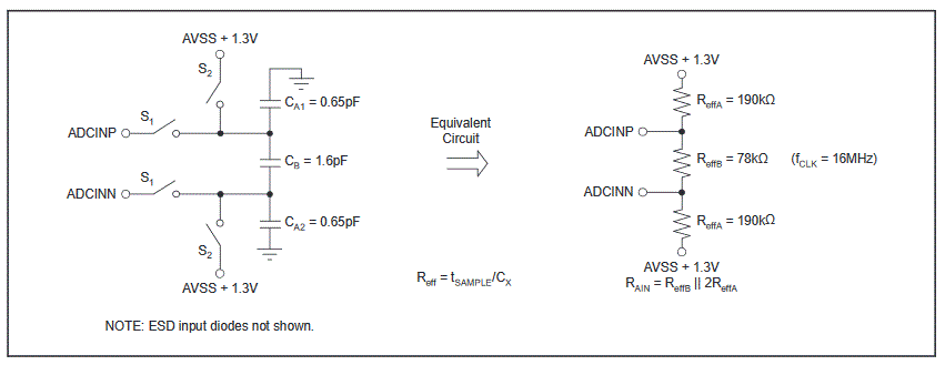
In the datasheet, it was stated that the differential input impedance is 65kohm. What is the typical ADC input resistance and charge capacitor value when the ADS1258 is configured to operate in single-ended mode?
Regards,
Carlo
Hi team,
Good day.
In the datasheet, it was stated that the differential input impedance is 65kohm. What is the typical ADC input resistance and charge capacitor value when the ADS1258 is configured to operate in single-ended mode?
Regards,
Carlo