This thread has been locked.

If you have a related question, please click the "Ask a related question" button in the top right corner. The newly created question will be automatically linked to this question.

ADS8528: REFAP/N, REFBP/N etc. and relation to REFIO

Part Number: ADS8528

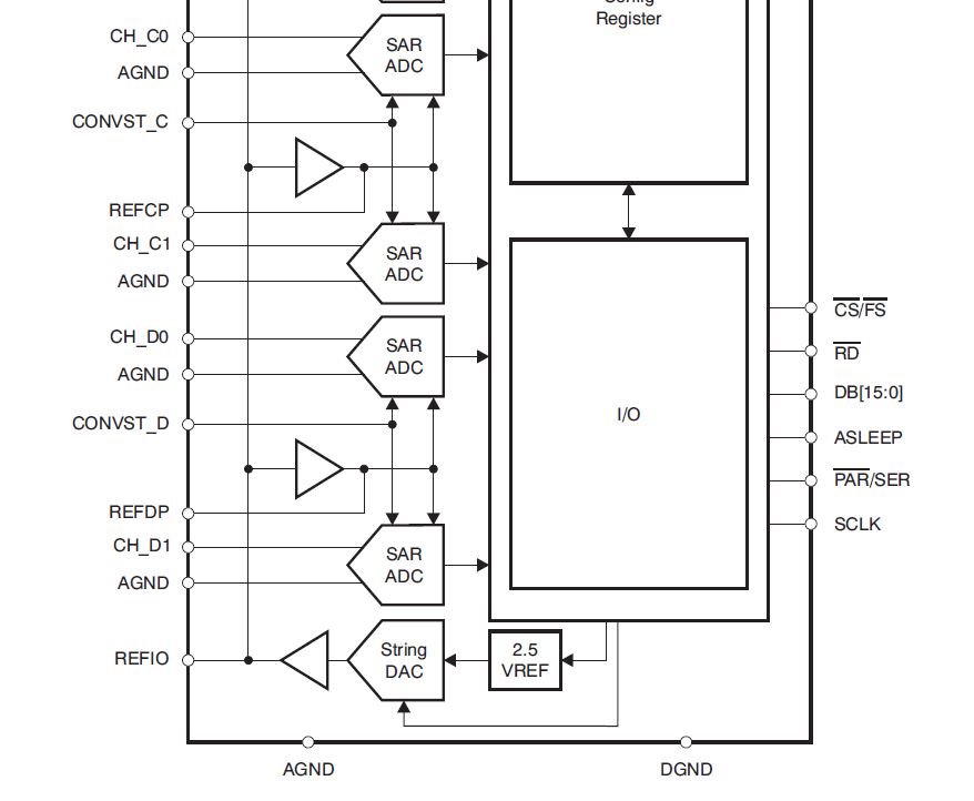
Hello, we are using ADS8528 in the hardware mode and we have the following connections:

REFIO: connected to external 2.5V via 33 Ohms and bypassed to AGND with 0.47u/50V/X7R

REFN: connected to AGND

REFAP, REFBP, ...: 10uF/10V/X7R capacitor to AGND

REFAN, REFBN, ...: connected to AGND

- The connections at REFAP etc. are made according to the datasheet. But it is not clear what the voltage at these pins should be? Is it the same voltage as the REFIO pin? Does having the 10uF capacitors at these pins capacitively load the external reference?

- Similar to ADS85x8EVM, we are driving the REFIO pin with an opamp. However, we have series resistor of 33 Ohms between the opamp's output and the 0.47u bypass capacitor at REFIO (to AGND). Is this better or worse than the EVM circuit? Is it alright to drive the 0.47u capacitive load directly from the opamp?

Thank you!

  • Hello Saurabh,

    Welcome to our forum and thank you for your post.

    The internal reference buffers A, B, C, and D should output the same voltage as the REFIO pin. The bypass capacitors on the REFxP pins are separated from the REFIO pin and will not load your external reference source.

    The REFIO pin is connected to the internal buffer at the output of the internal reference DAC. In addition, the REFIO pin connects to each of the four reference buffers (A, B, C, and D). The DAC reference buffer is powered-down by default, allowing you to drive an external 2.5-V reference voltage. The REFIO pin can be treated as a high-impedance input, so the 33 ohms in series and the 0.47-uF bypass capacitor is fine. In fact, you could increase the capacitor to 47 uF and low-pass filter more of the reference voltage noise.

    For reference, here is a portion of the internal functional block diagram in section 9.2:

    Regards,