We've just received our ADS1248 boards that measures 2 differential voltages (AIN0/AIN1, AIN4/AIN5) and 2 RTDs (AIN2/AIN3 , AIN6/AIN7 ). For testing, I've placed 1.5k resistors on the RTD inputs.
I've verified NRST & START pin are both high, and wait for NDRDY to go low before clocking (1.875 Mhz SCLK) the next channel setup while saving the MISO data containing the previous channel result.
For example, for the 2 RTD inputs, I've configured the chip's registers for all biases disabled, pga=1 , internal reference control on, IDAC0 1ma, and IDAC1 to source on AIN2, yet R35 shows only 0.01v.. I would expect 2v (1ma thru the 2K), See schematics below.
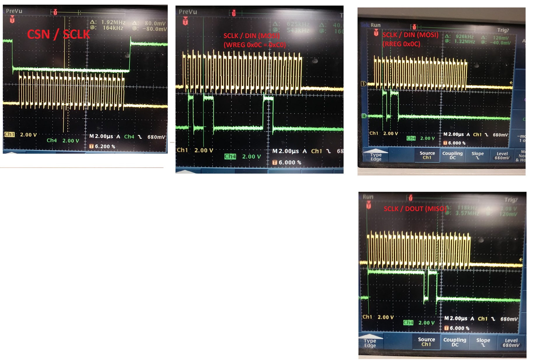
The SPI comm to the chip looks good, I see one long active-low Chip-Select for all 14 bytes on MOSI. However the data returned for the 1.5k RTD (retrieved on the next SPI transaction) is zero. The scope pictures below shows SCLK/CSN, and MOSI/SCLK for the first 4 bytes (of 14) when configuring the RTD channel (AIN2/AIN3) . These MOSI bytes are : 0x40 (WREG), 0xC (LEN), 0x13 (MUX AIN2/AIN3), 0x00 (Bias disable). As an experiment, I tried changing the PHAse polarity such that controller changes the data on the rising edge (instead of the falling edge), but didn't make any difference.
What could cause no current thru AIN2 and data (for all channels) to be zero?