This thread has been locked.

If you have a related question, please click the "Ask a related question" button in the top right corner. The newly created question will be automatically linked to this question.

Command order for DAC80004

Other Parts Discussed in Thread: DAC80004

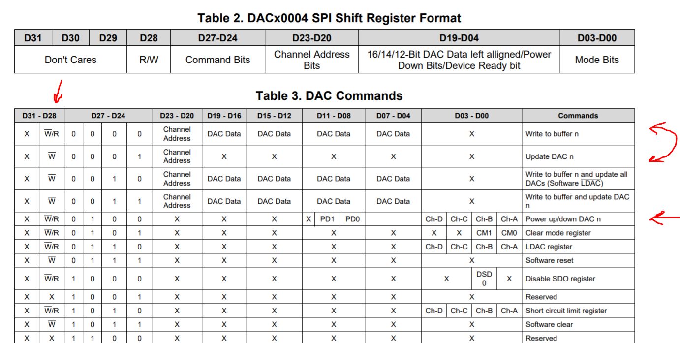
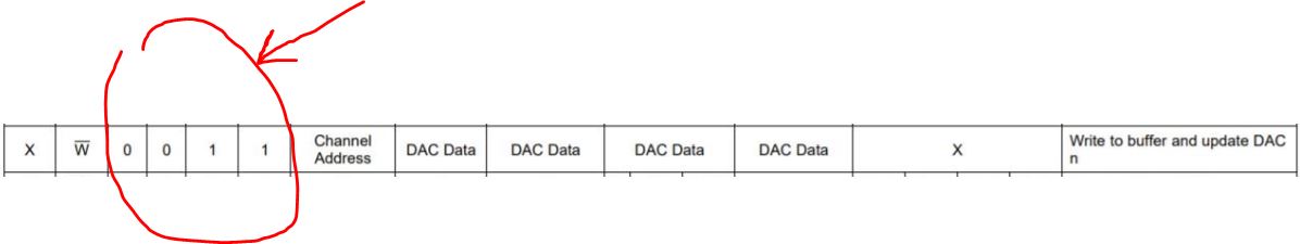
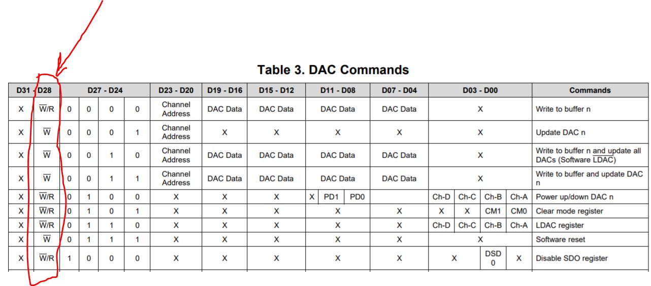
Hello, in the DAC80004 data sheet from the link shown bellow i cant see orders like power up power down,writing to a buffer ,updating the buffer.

So i guess there is some order of operation when i deal with DAC80004 .

Where can i see the full order of command on how to operate with dac80004

I can guess we need to power it on first then send write to buffer thenupdate dac then power off when we done.

Is there some order step by step command we we need to do ,in order to function it properly?

Thanks

https://www.ti.com/lit/ds/symlink/dac80004.pdf?ts=1596748188099

  • Hi Yefj,

    By default, all the channels are powered up.  You should determine if you need an configuration that is different than the default configuration.

    For example, if you do not want to use the LDAC pin, then you would need to update the LDAC register before writing the first value to the DAC buffer.

    Otherwise there are very few configuration options for this device.  Is there a specific use case you are concerned about?

    Thanks,

    Paul

  • Hello Paul,My goal is to write a digital data to DAC8004 and to see the  analog result in the output.

    I have here command write to buffer command,update dac command,power on dac command.

    Which one should i use for my goal?
    Thanks.

  • Hi Yefj,

    As Paul mentioned, By default all channels are powered up. Assuming you want to do synchronous updates( where LDAC pin is not required, permanently tie to ground), you can use the 4th configuration in the table you mentioned with command bits as 0011.

    If you want to use LDAC pin functionality by hardware toggle, use command bits 0000

    if you want to use software LDAC functionality, first set the LDAC mode by writing into LDAC register (command bits 0110) and then write using command bits 0010.

    Hope this clarifies, let me know if you need more help.

    Regards,

    AK

  • Hello Akhilesh, There is a command 32bit long  called "write to a buffer".if i send it to the DAC8004 via SPI will convert the digital data to analog signal?
    or i need the update DAC command too?
    Thanks.

  • Hi,

    If you just want to send  DAC data and update automatically (synchronous mode), use command bits 0011.

    Regards,

    AK

  • Hello,i cant send only 4 bits.

    I need to send the whole 32 bit command(8 bit at a time) shown bellow .Correct?

  • Hi,

    yes, you need to send 32bits.

    I mentioned only command bits for easy understanding. Without sending DAC data how can you expect to get output ?

    Regards,

    AK

  • Hello,regarding the SPI communication with DAC8004, is it set in such way that i need to send from my controller MSB first or LSB first?

    Thanks.

  • Hi Yefj,

    Data should be MSB first.

    Regards,

    AK

  • Hello, i could not find in the manual regarding the W/R.If want to use write buffer and update, What should be the W/R bit?

    Thanks.

  • Hi,

    If you see correctly, for write operation its '0' and for read its '1'. W has bar on top of it

    Regards,

    AK

  • Hello, I have assebled a coomand for the DAC80004,is it ok?

    from the MOSI (my microcontroller, given CS low) it will write the  0000 1111 1111 1111 digital data and convert it threw channel 1

    Correct?

    Thanks

    uint8_t B0_B7[8]=0b11110000; //first 4 are dont care,first 4 bits data
    uint8_t B8_B15[8]=0b11111111;//data bits
    uint8_t B16_B23[8]=0b00000000;//channel A DATA total 0000 1111 1111 1111
    uint8_t B24_B31[8]=0b0000011;//write to buffer and update DAC ,Write /rest dont care

  • Hi,

    These sequence looks good to me.

    Let me know if you need more help regarding the same.

    Regards,

    AK

  • Hello , i want that a copy of this command will be sent back to my controller straight away as it comes in.
    There is no SDO enable in the table bellow

  • Hi,

    Look at command to enable/disable SDO register (Command = '1000'. Please look at the readback timing diagram for reading data from SDO.

    Also SDIN data will not be clocked out on SDO, you need to do NOP command after giving the command for read operation.

    Also this SPI implementation is half duplex, not full duplex. 

    Regards,

    AK

  • Hello,So in the 1000 command W/R=0 because we are writing .
    in D3-D0: the DSD=1

    So i Send my command from controller to DAC80004

    then i do the 1000 command to enable readback
    and after the 1000 command i do the NOP

    Inside the NOP command W/R should be 1 or zero because we are not reading Or wrting in NOP?

  • Hi,

    Which register are you trying to readback? For NOP command, W/R should be zero.

    Regards,

    AK

  • Hello,In the DAC80004 diagram shown bellow I enter the commands threw SDIN and i expect the readback (a copy of my SDIN command) to go from SDO to my controller.

    First i send write update command then Enable SDO register and then NO Operation COMMAND
    for all three command i used W/R=0 as sown in the command bellow.

    did i do everything correctly?

    given that i sent these 3 commands ,the DAC80004 will SEND this command every clock cycle threw SDO of it will send it once?

    //start write update command
            uint8_t B7_B0[8]=0b11110000; //first 4 are dont care,first 4 bits data
         	uint8_t B15_B8[8]=0b11111111;//data bits
         	uint8_t B23_B16[8]=0b00000000;//channel A DATA total 0000 1111 1111 1111
         	uint8_t B31_B24[8]=0b00000011;//write to buffer and update DAC ,Write /rest dont care
         	//start end update command
    
         	uint32_t Recieved_D;
            //Enable SDO register
         	uint8_t C31_C24[8]=0b00001000; //enable DSO command
         	uint8_t C23_C16[8]=0b00000000;
         	uint8_t C15_C8[8]=0b00000000;
         	uint8_t C7_C0[8]=0b00000010;// enable DSO bit
    
         	//NO OPeration COMMAND
         	uint8_t D31_D24[8]=0b00001110;
         	uint8_t D23_D16[8]=0b00000000;
         	uint8_t D15_D8[8]=0b00000000;
         	uint8_t D7_D0[8]=0b00000000;

  • Hi,

    Code looks fine to me. Keep in mind that SDO will have data in the NOP command frame.

    Regards,

    AK

  • " Keep in mind that SDO will have data in the NOP command frame."
    OK so my data will be in  the form shown bellow.

    The readback  sends a copy of the command from SDIN to SDO goes once? or every few seconds?

    Thanks.

  • Hi,

    Please see the below timing diagram for better explanation.

    First give read command and then issue a NOP command. You will get the requested data in second frame.

    Regards,

    AK

  • Hello, Till now i thought i need to do the following procedure for readbakc

    Write and update-> enable sdo->NOP (3 command)

    Now you say i should do

    Write and update-> enable sdo->read->NOP(4 commands)

    but in the command table there is no "read command",how "read command" called in the table of DAC commands?

    maybe you mean the 0000 command but W/R=1 ?

  • Hello Akhilesh,Whar is the read command i cant see it in the table

  • Hi,

    I think you didn't understand what i conveyed earlier. Let me clarify.

    For reading any register, you need 2 SPI frame. First frame, you send the read command for reading from a particular register, and then issue a NOP command.

    Example : 

    You need to read the DATA register, procedure will be as follows. (This is for reading, I am assuming you already wrote into the DATA register and enabled SDO for readback, this should be done initially)

    1. First send the read command with command bits 0000 with W/R set to 1, give the address of the channel you want to read, other bits are don't care ( can be '0' or '1')

    2. Send the NOP command with command bits 1110, R/W set to '0', other bits are don't care again

    3. You will get the requested data in SDO, in the second frame.

    Hope this clarifies. Also please use this thread to follow up, no need to open new threads for the same issue.

    Regards,

    AK

  • Hello ,I did exactly as you said.i use manual CS for my SPI so i put CS to low, give the send command and then raise the CS high in the end.

    i have tried to write in channel A 0000  the data 0000 1111 1111 1111 1111

    i put the recieved uint32 into a UART transmission to see what i get. and i dont get the data i put in the command. as shown in the transmission bellow.

    Also my recieved uint32 is initialised as all 1's and clearly i dont get this initial value too ,i get some result i dont know how to interpet.
    I have attached my full code.
    Why iget this weird result?
    Thanks.


    #include "em_device.h"
    #include "em_cmu.h"
    #include "em_gpio.h"
    #include "spidrv.h"
    #include "dmadrv.h"
    #include "em_usart.h"
    #include "em_chip.h"
    #include <stdint.h>
    #include <stdbool.h>
    #include "em_emu.h"
    
    #include "bsp.h"
    #include "bsp_trace.h"
    #define LED_PORT_E    gpioPortE
    #define LED_PIN_E     15
    
    #define LED_PORT_A    gpioPortA
    #define LED_PIN_A     15
    
    #define USER_LOCATION 5
    
    #define BUFFER_SIZE 1
    char buffer[BUFFER_SIZE];
    
    volatile uint32_t msTicks; /* counts 1ms timeTicks */
    
    void Delay(uint32_t dlyTicks);
    void SysTick_Handler(void)
    {
      msTicks++;       /* increment counter necessary in Delay()*/
    }
    void Delay(uint32_t dlyTicks)
    {
      uint32_t curTicks;
    
      curTicks = msTicks;
      while ((msTicks - curTicks) < dlyTicks) ;
    }
    int main(void)
    {
    
    //	uint8_t *pt;
      int i,j;
       i=0;
            //start write update command
            uint8_t B7_B0=0b11110000; //first 4 are dont care,first 4 bits data
         	uint8_t B15_B8=0b11111111;//data bits
         	uint8_t B23_B16=0b00000000;//channel A DATA total 0000 1111 1111 1111
         	uint8_t B31_B24=0b00000011;//write to buffer and update DAC ,Write /rest dont care
         	//start end update command
    
         
         	uint32_t Recieved_D=0b11111111111111111111111111111111 ;
            //Enable SDO register
         	uint8_t C31_C24=0b00001000; //enable DSO command
         	uint8_t C23_C16=0b00000000;
         	uint8_t C15_C8=0b00000000;
         	uint8_t C7_C0=0b00000010;// enable DSO bit
    
         	//NO OPeration COMMAND
         //	uint8_t D31_D24=0b00001110;
         //	uint8_t D23_D16=0b00000000;
         //	uint8_t D15_D8=0b00000000;
         //	uint8_t D7_D0=0b00000000;
    
    
         	 //start read command 0000
         	        uint8_t E7_E0=0b11110000; //first 4 are dont care,first 4 bits data
         	     	uint8_t E15_E8=0b11111111;//data bits
         	     	uint8_t E23_E16=0b00000000;//channel A rest is dont care
         	     	uint8_t E31_E24=0b00010000;//read
         	     	//start end update command
    
         	     	//NO OPeration COMMAND
         	     	     	uint8_t F31_F24=0b00001110;
         	     	     	uint8_t F23_F16=0b00000000;
         	     	     	uint8_t F15_F8=0b00000000;
         	     	     	uint8_t F7_F0=0b00000000;
      // Chip errata
      CHIP_Init();
    
      // Enable oscillator to GPIO and USART1 modules
      CMU_ClockEnable(cmuClock_GPIO, true);
      CMU_ClockEnable(cmuClock_USART1, true);
      CMU_ClockEnable(cmuClock_USART0, true);


    //  BSP_TraceProfilerSetup();
    
        /* Setup SysTick Timer for 1 msec interrupts  */
        if (SysTick_Config(CMU_ClockFreqGet(cmuClock_CORE) / 1000)) {
          while (1) ;
        }
    
        /* Initialize LED driver */
    
      //  BSP_LedsInit();
      //  BSP_LedSet(0);
      // set pin modes for UART TX and RX pins
      GPIO_PinModeSet(gpioPortC, 1, gpioModeInput, 0);
      GPIO_PinModeSet(gpioPortC, 0, gpioModePushPull, 1);
      ///////////////////////////////////
        USART_InitAsync_TypeDef init = USART_INITASYNC_DEFAULT;
        USART_InitAsync(USART1, &init);
        //defining location 0 so PORT C will be tx an rx for async uart
        USART1->ROUTE |= USART_ROUTE_TXPEN | USART_ROUTE_RXPEN|USART_ROUTE_LOCATION_LOC0;
       // GPIO_PinModeSet(LED_PORT_A,15,gpioModePushPull,1);
    
          GPIO_PinModeSet(LED_PORT_E,15,gpioModePushPull,1);
    
        GPIO_PinModeSet(LED_PORT_A,2,gpioModePushPull,1);
        SPIDRV_HandleData_t handleData;
      	SPIDRV_Handle_t handle = &handleData;
      	SPIDRV_Init_t initData =  SPIDRV_MASTER_USART0;
      	initData.csControl=spidrvCsControlApplication; //manual CS
      	initData.bitOrder=1; //MSB first send bit order
      	initData.portLocation = USART_ROUTE_LOCATION_LOC0; //defining location 0 for sync uart
      	SPIDRV_Init(handle,&initData);
    
      	GPIO_PinOutClear(LED_PORT_A,2); //chip select low starts transmition
      	SPIDRV_MTransmitB(handle, &B31_B24, 1);
      	SPIDRV_MTransmitB(handle, &B23_B16, 1);
      	SPIDRV_MTransmitB(handle, &B15_B8, 1);
      	SPIDRV_MTransmitB(handle, &B7_B0, 1);
      	GPIO_PinOutSet(LED_PORT_A,2); // chip select high,end transmition
      	 Delay(1000);
    //////////////////
      	GPIO_PinOutClear(LED_PORT_A,2); //chip select low starts transmition
      	SPIDRV_MTransmitB(handle, &C31_C24, 1);
      	  	SPIDRV_MTransmitB(handle, &C23_C16, 1);
      	  	SPIDRV_MTransmitB(handle, &C15_C8, 1);
      	  	SPIDRV_MTransmitB(handle, &C7_C0, 1);
      	  GPIO_PinOutSet(LED_PORT_A,2); // chip select high,end transmition
      	Delay(1000);
      	//////////////
      	GPIO_PinOutClear(LED_PORT_A,2); //chip select low starts transmition
      	   	    	SPIDRV_MTransmitB(handle, &E31_E24, 1);
      	    	  	SPIDRV_MTransmitB(handle, &E23_E16, 1);
      	    	  	SPIDRV_MTransmitB(handle, &E15_E8, 1);
      	    	  	SPIDRV_MTransmitB(handle, &E7_E0, 1);
      	    	//////////////
      GPIO_PinOutSet(LED_PORT_A,2); // chip select high,end transmition
      Delay(1000);
      GPIO_PinOutClear(LED_PORT_A,2); //chip select low starts transmition
      	    	  SPIDRV_MTransmitB(handle, &F31_F24, 1);
      	    	    	    	  	SPIDRV_MTransmitB(handle, &F23_F16, 1);
      	    	    	    	  	SPIDRV_MTransmitB(handle, &F15_F8, 1);
      	    	    	    	  	SPIDRV_MTransmitB(handle, &F7_F0, 1);
      	GPIO_PinOutSet(LED_PORT_A,2); // chip select high,end transmition
    
      // Initialize USART asynchronous mode and route pins


      	GPIO_PinOutClear(LED_PORT_A,2);
      	 SPIDRV_MReceiveB(handle,&Recieved_D,4);
      	GPIO_PinOutSet(LED_PORT_A,2);
    
      	uint8_t * pt = (uint8_t*)(&Recieved_D);
    
          while (1)
         {
    
    //E-green
    //A-red
    
        	  Delay(1000);
    
    
        	     for (i = 0; i < 4 ; i ++ )
        	         {
        	    	 USART_Tx(USART1,*(&Recieved_D+i));
        	    	 USART_Tx(USART1,*(pt++));
        	         }
        	         USART_Tx(USART1, '\n');
        	         GPIO_PinOutClear(LED_PORT_E,15);
        	   	  Delay(5000);
        	   	  GPIO_PinOutSet(LED_PORT_E,15);
        	   	Delay(5000);
          }//end while(1)
      }//end main


  • Hi,

    I am not a software person to look for error in the code, as I am not qualified to do so.

    Please follow the procedure, I have outlined in the above post, and you should be able to read back the data.

    Did you raise the SYNC(CS) after the first frame? You need to to do that before sending the NOP command. Please see the timing diagram in datasheet for readback.

    Regards,

    AK

  • So for each command i separatly  lower at start and raise in the end my CS

    in order to write:

    i use write and update command-> DSO enable command

    in order to read:

    0000 command with W/R=1 to see the value at some channel->NOP command

    and i get the data threw SDO.

    Correct?

    Also i get All zero recieved.is it possible?

  • Hi,

    The sequence is fine, First write some data into channel, by default all data registers will be loaded with zeros, probably you are reading that.

    Can you post the scope shots for your SPI frame?

    Regards,

    AK

  • Hello Akhilesh,I  am working on producing the signal's on Scope.

    In the bellow diagram you can see how my dac80004 is connected.
    How is LDAC and POR should be connected so i could send the SPI command and see the analog  voltage from Vout A  for example?
    Thanks.  

  • Hi,

    What kind of updates are you looking at? do you need synchronous or asynchronous update?

    In synchronous mode, data are updated with the falling edge of the 32nd SCLK cycle, which follows a falling edge of SYNC. For such synchronous updates, the LDAC pin is not required, and it must be connected to GND permanently or asserted and held low before sending commands to the device.

    In asynchronous mode, the LDAC pin is used as an active low signal for simultaneous DAC updates. After a LDAC low pulse, all DACs are simultaneously updated with the last contents of the corresponding data buffers. If the content of a data buffer is not changed, the corresponding DAC output remains unchanged after the LDAC pin is pulsed low.

    Regarding POR pin, if its grounded, upon power up data registers will be loaded with all zeroes, resulting in zero output at power up. If POR pin is connected to VDD, data registers are loaded with mid code, and output will be mid scale upon power up.

    Hope this clarifies your query.

    Regards,

    AK

  • Hello Akhilesh, I am working in synchronous mode, so based on what you say  LDAC has to be low.
    regarding the POR as you can see in the diagram its connected to GND,So will it block my write and update command from changing the value of the DAC ?
    or POR has a wrole only in startup phase and the SPI command will be the dominant?
    Thanks.

  • Hi,

    Yes, LDAC has to be low on power up or you can permanently tie to ground.

    POR is Power on Reset. It will not block your write operation. The DACx0004 contain a power-on-reset circuit that controls the output voltage during power up. The power-on reset is useful in applications where it is important to know the state of the output of each DAC while the device is in the process of powering up. At power up all DAC registers are filled with power-on reset code

    This will not block your SPI write.

    Regards,

    AK

  • Hello ,regarding the CLEAR pin, Is it suposseded to be 0 or VDD logic in order that my SPI command will be recieved?
    Thanks.

  • Hi,

    CLR pin is active low. So for normal operation, it should be high.

    Regards,

    AK

  • Hello, i am trying to send the  0000 0011 0000 1111 1111 1111 1111 0000 . so i could write the maximal voltage on channel 0.
    As you can see in the photos bellow i showed the signals VS one another (only have two channels in my scope)
    CLR=1 LDAC=0 

    CLOCk=1MHz.
    What do you think about the signal patterns ?(i noticed that SYNc rises right in the middle of my command) is it a problem?

    Do you think i at least made the correct SDIN pattern?
    Thanks.

  • Hi,

    As I mentioned in other thread which is opened by you, SYNC has to stay low for 32 clocks to recognize as one SPI frame.

    You cannot have SYNC transition  before completion of one SPI frame, in which case SPI frame will be invalid. Its called SYNC interrupt.

    SYNC line stays low for at least 32 falling edges of SCLK and the addressed DAC register updates on the 32nd SCLK falling edge. However, if SYNC is brought high before the 32nd SCLK falling edge, it acts as an interrupt to the write sequence; the shift register resets and the write sequence is discarded. Neither an update of the data buffer contents, DAC register contents, nor a change in the operating mode occurs

    Regards,

    AK

  • Hi,

    I have already replied the same in another thread which you have  opened. I am closing this thread and we an continue the discussion there.

    Regards,

    AK

  • Hello i am using 3 commands, with LDAC=0 CLR=1

    First command:

    //W/R=0 write and update channeL0 all1 data dont cate
    // {00000011,b00001111,11111111,11110000}; channel 0(register 0) write FFFF expect to get full scale VDD
    {0x03,0x0F,0xFF,0xF0};

    1ms delay

    Second command:

    enable DSO second bit is one to enable,{0x08,0x00,0xFF,0x02}

    1ms delay

    third command:

    NOP command

    {0x0E,0x00,0x00,0x00}

    As i understand a channel is a register so when  i defined all '1' in channel 0 with write and update i command,when i read i need to get all '1' data but 

    after those three I get absolutly no response in the SDO straight zero?

    I have attached bellow enumirate photos of step by step data vs CLK ,in every command

    DATA vs sync

    Where did i go wrong?
    Thanks.

  • Hi,

    As I mentioned in other thread, I am closing this, we will follow up in the other thread which you have opened for the same issue.

    Please don't reopen the same.

    Regards,

    AK