Other Parts Discussed in Thread: ADS1299, ADS1298
Hello team,
We have started testing the ADS1299 EVK and are stuck onto an issue.
The input configuration used here is single ended input
Jumper settings of the EVK are as follows:
1. JP7: no jumper
2. JP8: 2-3
3. No jumpers at JP25 (1-2, 3-4, 5-6)
The other jumpers are as per the factory default settings wherein the board is running on an unipolar supply.
I have provided positive input from the signal generator to pin 36 of J6 (channel one positive)
And the Ground of the signal generator is connected to pin 6 of JP25.
The input from the signal generator is a sine wave of frequency 1Hz, amplitude being 100mVp-p.
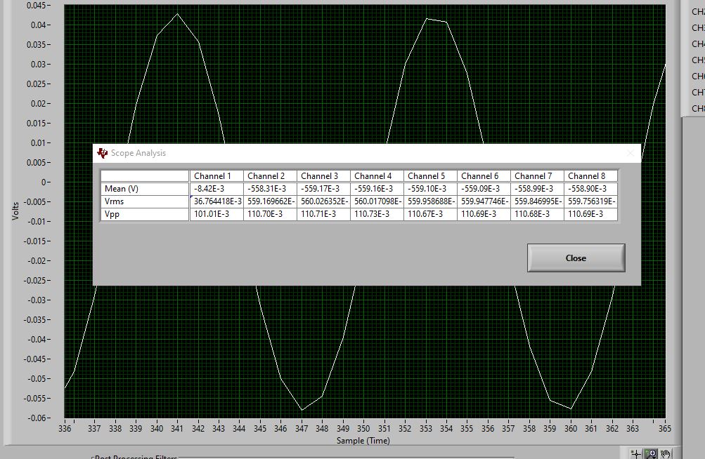
The waveform acquired is as below:
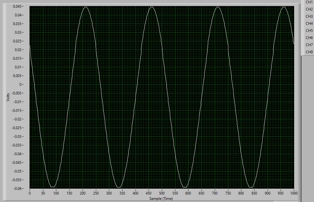
Scope analysis :

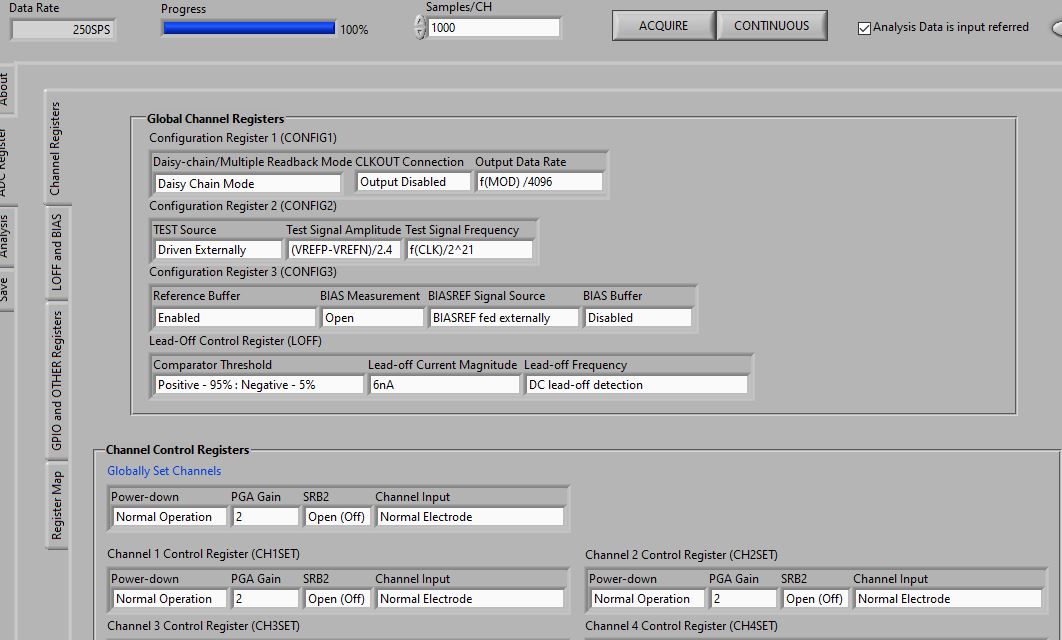
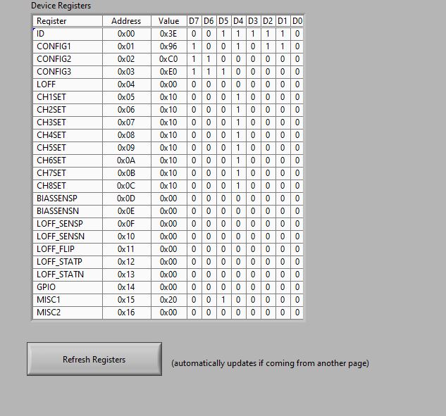
Register settings:


The issue here are:
1. The amplitude set is 100mV. However I am getting 103.9mV. How can I attain the accuracy required?
I have tried using the external reference buffer and also tried to increase the gain, the amplitude however was unchanged.
2. If at all you see the waveform, it is clipped for the negative edge. Even though the amplitude measured is more than the input signal, the representation is a clipped wave. Is it normal or an actual issue?
3. I can see some voltages on other channels too. Currently there is no input on other channels except channel 1. Why are the voltages appearing on the other channels?
Kindly confirm if the register settings are correct for single ended input.
Also, if I increase the frequency of the input signal, the waveform gets more distorted. Please help me knowing why is it so.
The waveforms for a 20Hz signal is attached below. Rest of the signal parameters and the EVK settings are unchanged:

My aim here is to use do the measurement as referential montage with the highest accuracy possible. Any inputs to achieve the same would be appreciated.
Thanks,
Sushant