A related question is a question created from another question. When the related question is created, it will be automatically linked to the original question.
If you have a related question, please click the "Ask a related question" button in the top right corner. The newly created question will be automatically linked to this question.
ADS124S08: ch-to-ch offset variation and ch-to-ch offset drift variation
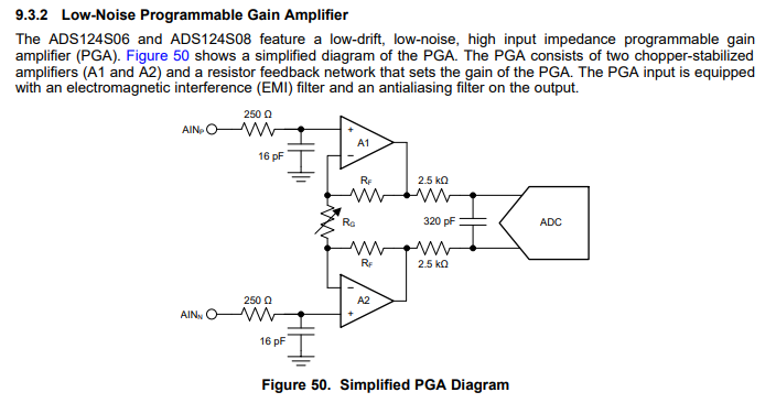
The ADS124S08 offset and offset drift is based on the selected AINP and AINN inputs and not specific to any mux channel inputs. The offset and offset drift characteristics would include the mux as there is no way to directly connect to the PGA/ADC any other way. The electrical characteristics table would apply to any selected input channel.
I know that the datasheet specifies offset/offset drift values for any combination of AINx. I think offset and offset drift value are different for each combination. For example these values of AIN1/AIN2 and AIN3/AIN4 are different. Is this correct?
But you don't have any data for how these values are different between each combination. Is this correct?
Are these values of a combination like AIN1/2 and these values of another combination like AIN3/4 completely different? One could go to positive value and another could go to negative value? For example, AIN1/2: offset = 2uV, offset drift = 100nV/C --> positive side AIN3/4: offset = -2uV, offset drift = -100nV/C ---> Negative side Could this kind of thing happen? I think the value could be different but could all combination go to the same direction(plus/minus) ?
What makes the AIN1/AIN2 input combination different than AIN3/AIN4 are switch connections. The offset and offset drift components are primarily the PGA and ADC modulator stages. So my question to you is how does a switch affect the offset? Would you have the same concerns using an external switch, such as an external mux or relays?
As far as reversing input combinations, the input is chopper stabilized. To remove any offset effect of the ADC you could use the global chop mode which will remove ADC offset by taking two measurements with one measurement swapping the inputs and then averaging the two values together.
What I am saying is there shouldn't be any measurable difference for any input combination on a single ADS124S08 device. There may be device to device variation and lot to lot variation, but within a single-device the construction is the same for each input channel. Offset will be determined by the PGA and ADC itself and not the input connections.
What may be the true concern by the customer is how the leakage/bias currents may affect measurement error with respect to input filter resistances. The leakage/bias currents would also be the same for each channel, but external resistances may cause error if the resistance is very large. This would be especially true if the PGA is bypassed. We have included graphs of the input current characteristics in the datasheet in Figures 8 through 15.
The ADS124S08 is designed to have equal channel characteristics which may not be true for all devices. One such example is the ADS1220 where the input bias/leakage current is much different with respect to input channel selection. The design of the ADS1220 has a low-side switch connection on the AIN3 input. The leakage on the AIN3 input is greater at higher operating temperatures due to device sizing to keep the low-side switch resistance low. In turn the leakage on this AIN3 pin is larger. The ADS124S08 also has a low-side switch but the position of the switch differs greatly between devices to eliminate the effect on the analog input channels.
So it would be helpful to fully understand the customer's concerns and what issues the customer has seen previously to create these concerns.