Because of the Thanksgiving holiday in the U.S., TI E2E™ design support forum responses may be delayed from November 25 through December 2. Thank you for your patience.

This thread has been locked.

If you have a related question, please click the "Ask a related question" button in the top right corner. The newly created question will be automatically linked to this question.

Sync rules for SPI command in DAC80004

Other Parts Discussed in Thread: DAC80004, DAC80004EVM

Hello, Regarding the SYNC (CHip Select)  laws of Dac80004.
1.What is the Maximal amount bits I can send over MOSI for a single Low Sync(Chip select) session?
2.What is the minimal amount of time SYNC (Chip select) has to be high in order for the DAC to recognise that the SPI sesion is OVER?
3.If i Send my 32 bit command in 4 different 8bit Sync sessions,will the Dac recognise it as a valid command of 32bits?

Thanks. 

www.ti.com/.../dac80004.pdf

  • Hi,

    Please find my answers inline.

    1.What is the Maximal amount bits I can send over MOSI for a single Low Sync(Chip select) session?

    I mean you wanted to ask how many commands you can send by keeping SYNC low, right? its one SPI command per frame. That means 32 bits

    2.What is the minimal amount of time SYNC (Chip select) has to be high in order for the DAC to recognize that the SPI session is OVER?

    35nS

    3.If I Send my 32 bit command in 4 different 8bit Sync sessions, will the DAC recognize it as a valid command of 32bits?

    No, SYNC has to stay low for one complete SPI frame ( that is for 32 bits)

    Regards,

    AK

  • Hi,

    Any update on this issue? Do you need more help?

    Regards,

    AK

  • Hello :-) thank you for remmembering.
    I am currently working on another device and i hope i get a good SPI signal to shown you as soon a possible regarding the DAC80004.
    Thanks again for remmembering.

  • Hi,

    Will wait for your scope shots and updates.

    Regards,

    AK

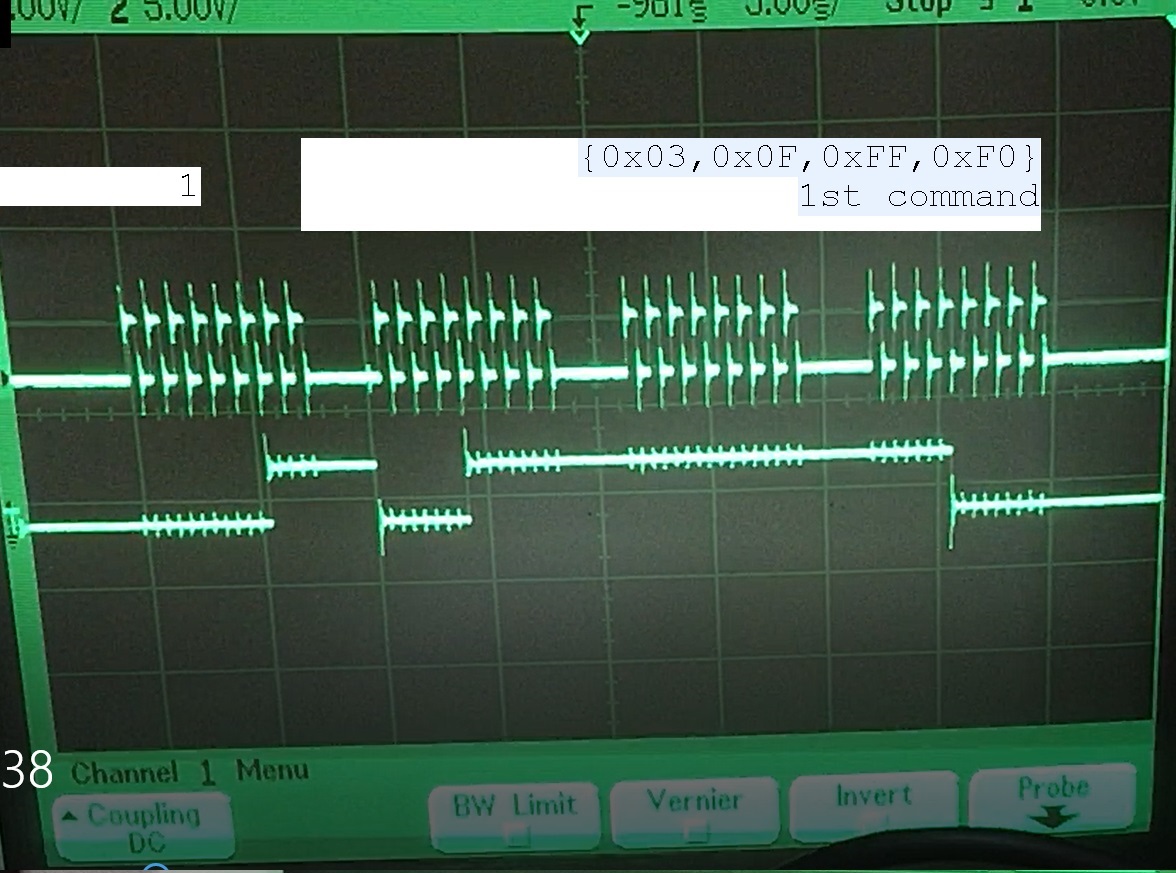
  • LDAC=0 CLR=1

    //W/R=0 write and update channeL0 all1 data dont cate
    // {00000011,b00001111,11111111,11110000}; channel 0(register 0) write FFFF expect to get full scale VDD
    first command {0x03,0x0F,0xFF,0xF0}

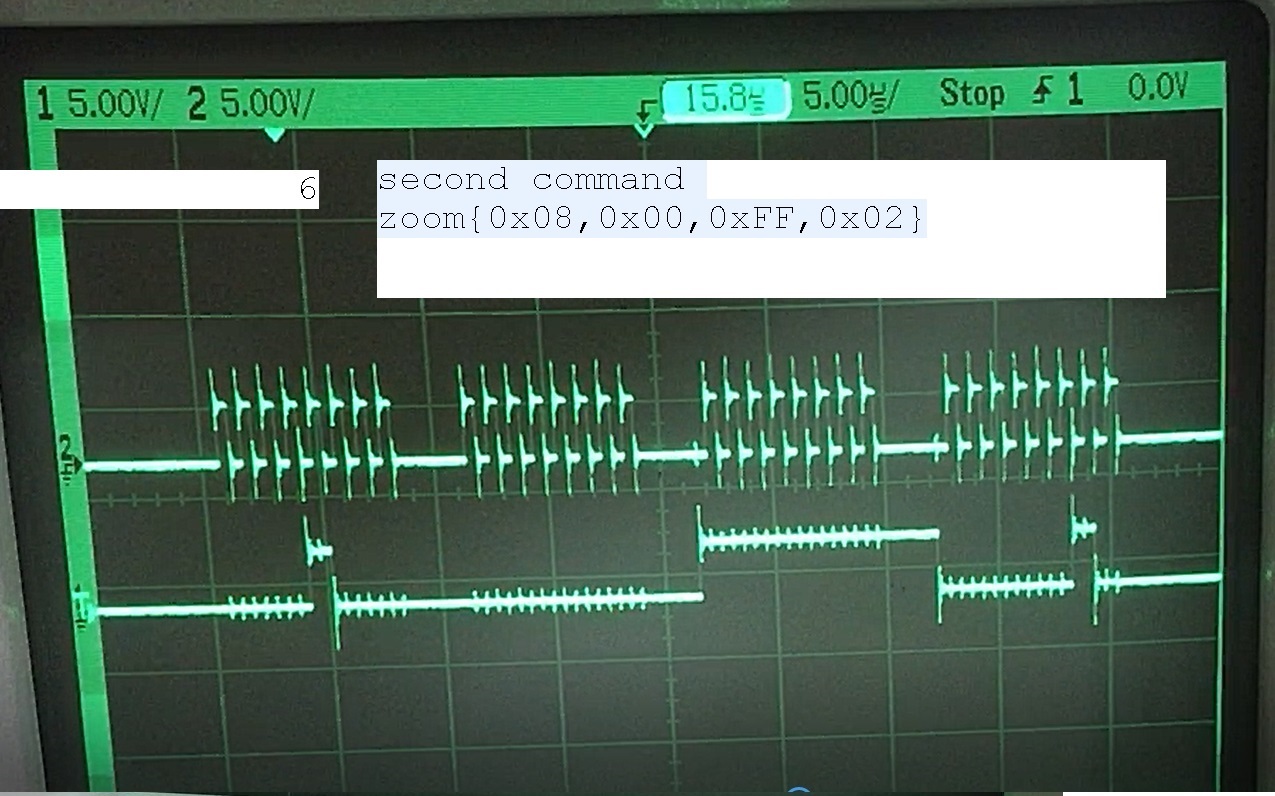
    Second command: enable DSO second bit is one to enable {0x08,0x00,0xFF,0x02}

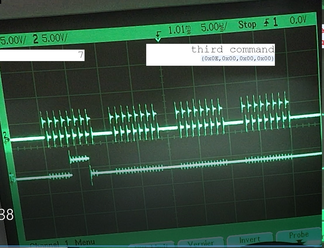
    third command:NOP command {0x0E,0x00,0x00,0x00}

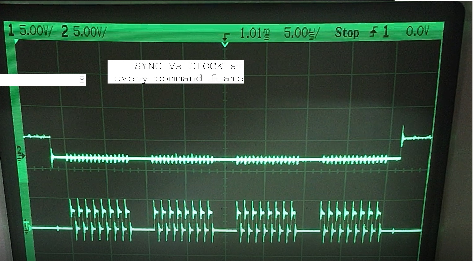
    I am sending my command in 8bits peaces so as you can see that is a gap in clock signal between subtransmitions,but as i understood its not a problem as long as SYNC is low.

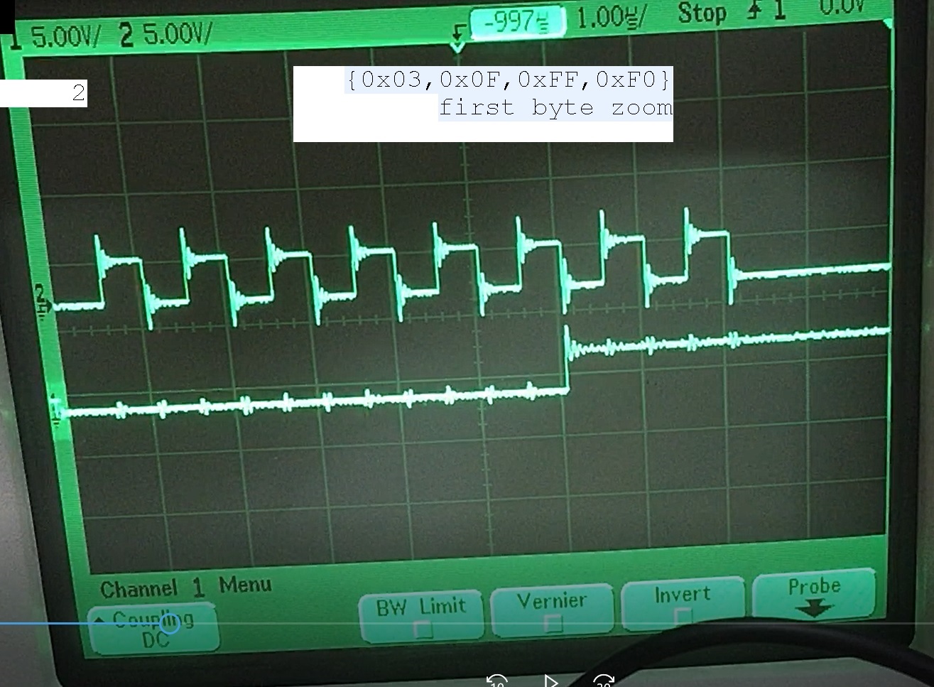
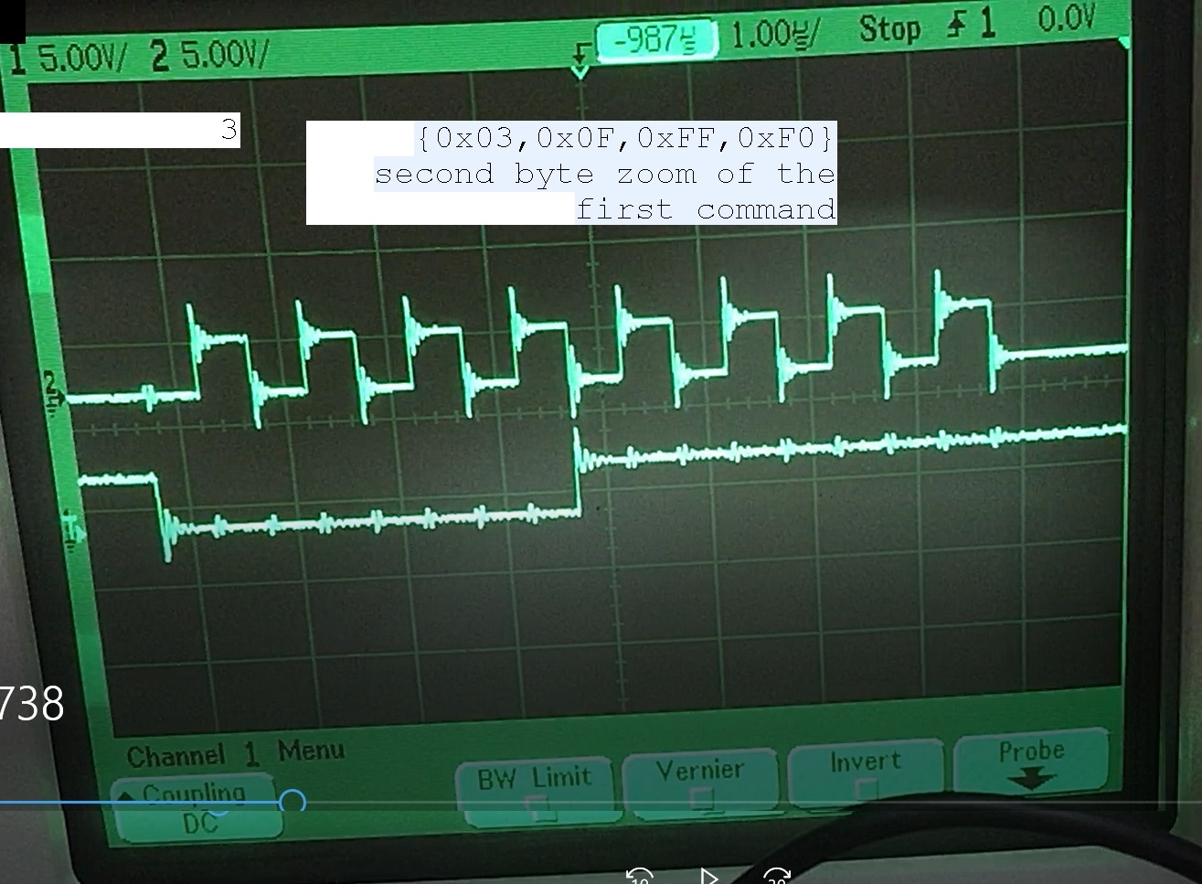
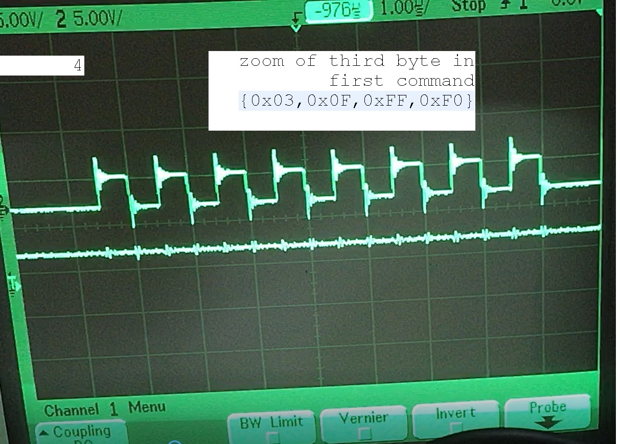
    I have attached the SDIN vs CLK in every command in a description in them with step by step enumiration
    I dont get any output at SDO i am supposed to get the data i put at the channel0 register which is all 1,but i get 0 response.

    Where did i go wrong?

  • Hi,

    These data frames looks fine to me. Whats the SPI clock frequency here?

    Also can you try without any gap between the SPI Clocks if possible?

    Please don't repost the same in the other thread, we will continue this discussion here, I will close the other thread, it creates unnecessary confusion for me.

    Regards,

    AK

  • the clock is 1Mhz. is it ok?

  • Hi,

    One more question, are you facing issues with read only or you are not able to get the DAC outputs working?

    Please share SDO frame as well for better understanding of the read frame. I want last two frames together in scope shot, meaning for reading you will send two frames, one will be read frame and second will be NOP frame

    Regards,

    AK

  • Hello Akhilesh,I will send the printscreens of scope as soon as possible.
    I have a fundamental question:
    is it ok with the device to send a comand in 8 bit peaces when CS is low the whole time and there is a small clock stop between 8bit packet transfer as shown bellow?
    Thanks.

  • Hi,

    No issues, you can send command like 4 packets of 8 bits with SYNC held low.

    Regards,

    AK

  • Hello this is the sequence of commands shown bello:

    1st command:

    W/R=0 write and update channeL0  all1 data    dont cate

    second command:

     {0x08,0x00,0xFF,0x02}

    Third NOP command
     {0x0E,0x00,0x00,0x00};

    4th command:

    just to generate clock for the device to respond:

    On each screen we have yellow-CLK turcqoise(middle one)-SDIN purple-SYNC
    I added a 4th command of all zerros just to generate clock to see the reaction from SDO,after it the SYNC rises back(scope zoom didnt capture it but its there if we move more to the right)

    I dont get Any SDO response whatsoever,I am starting to think this component is just burned,because the challel 0 output has no voltage ,the SDO clear all the time no response

    my CLR*=3.3v my LDAC*=0.

    Is it safe to assume that the component is burned ?
    Thanks.


  • Hi,

    One simple question, are you able to configure the device and get output? 

    For read back you don't need to send 4 commands. just send the read command and NOP command, in the second NOP frame SDO will have the data you have requested in the first frame.

    Just breakdown problem and try to solve. Let me know which is your read command in the pics above, is it the third command? if yes, why are you giving more than 32 clks while SYNC is low?

    Regards,

    AK

  • I will try again in the EVB board.

    Do you atleast agree that i shoould have got voltage vdd at channel 0 after the 1st command?

  • Hi,

    Your first command for getting the full code output on Channel A will be as follows. ( I assume this is the data you sent, not clear from your scope shots)

    0x03, 0x0F, 0xFF, 0xF0

    What are your clock phase and polarity settings for your MCU? I cannot quite make out the timing due to the scale of the plots, but it looks like data is changing on SDIN at around the same time as the falling clock edge.

    Data is shifted into the device on the falling edge of SCLK, so there is some risk that invalid or unintended data is being latched and therefore you are not seeing the desired results at the output. Generally speaking for a falling edge critical interface I would expect to see data change on the rising edge so that setup and hold timings are met, so maybe your fix is as simple as changing CPOL and CPHA settings for the SPI.

    Regards,

    AK

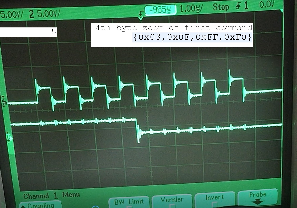
  • Hello, I have made a more clear photos when i sent only the first command

    {0x03,0x0F,0xFF,0xF0}
    1.am i supposed to see VDD on channel 0?

    2.from the photos shown bellow,do you still say i have a clock problem?I will try the same SPI sequence on The DAC80004EVM it will not work there too?

    Thanks.

  • Hi Yefj,

    Seems like your SPI clock is inverted.  The DAC80004 requires data to be set up on the rising edge and latched on the falling edge.

    Thanks,

    Paul

  • Yes worked perfectly,thanks.