Dear Experts,
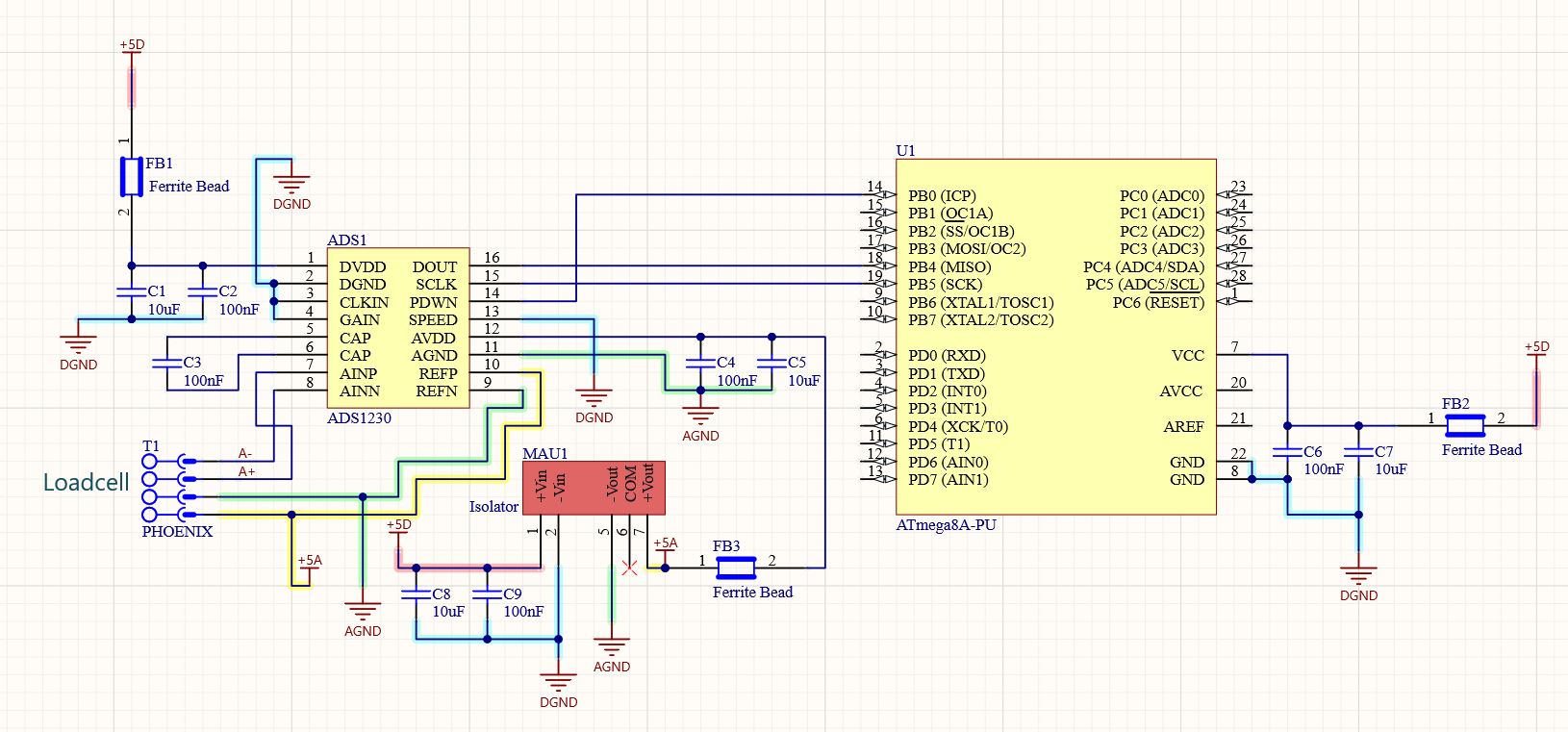
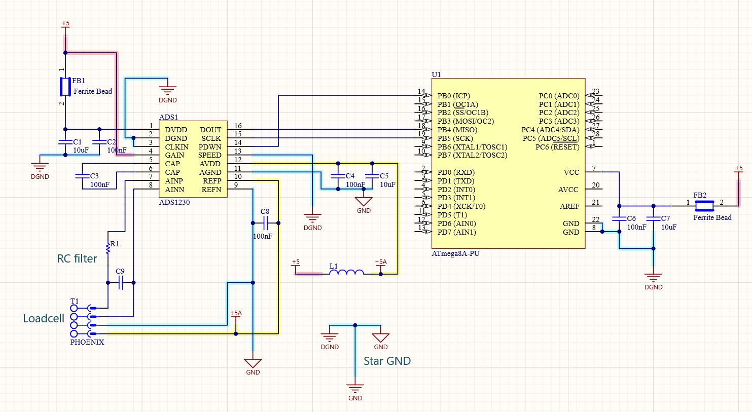
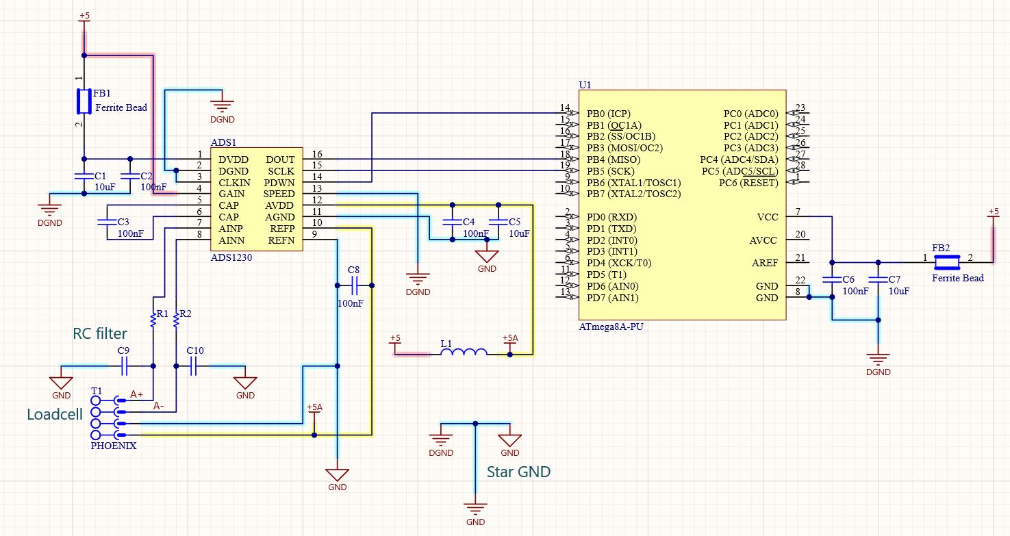
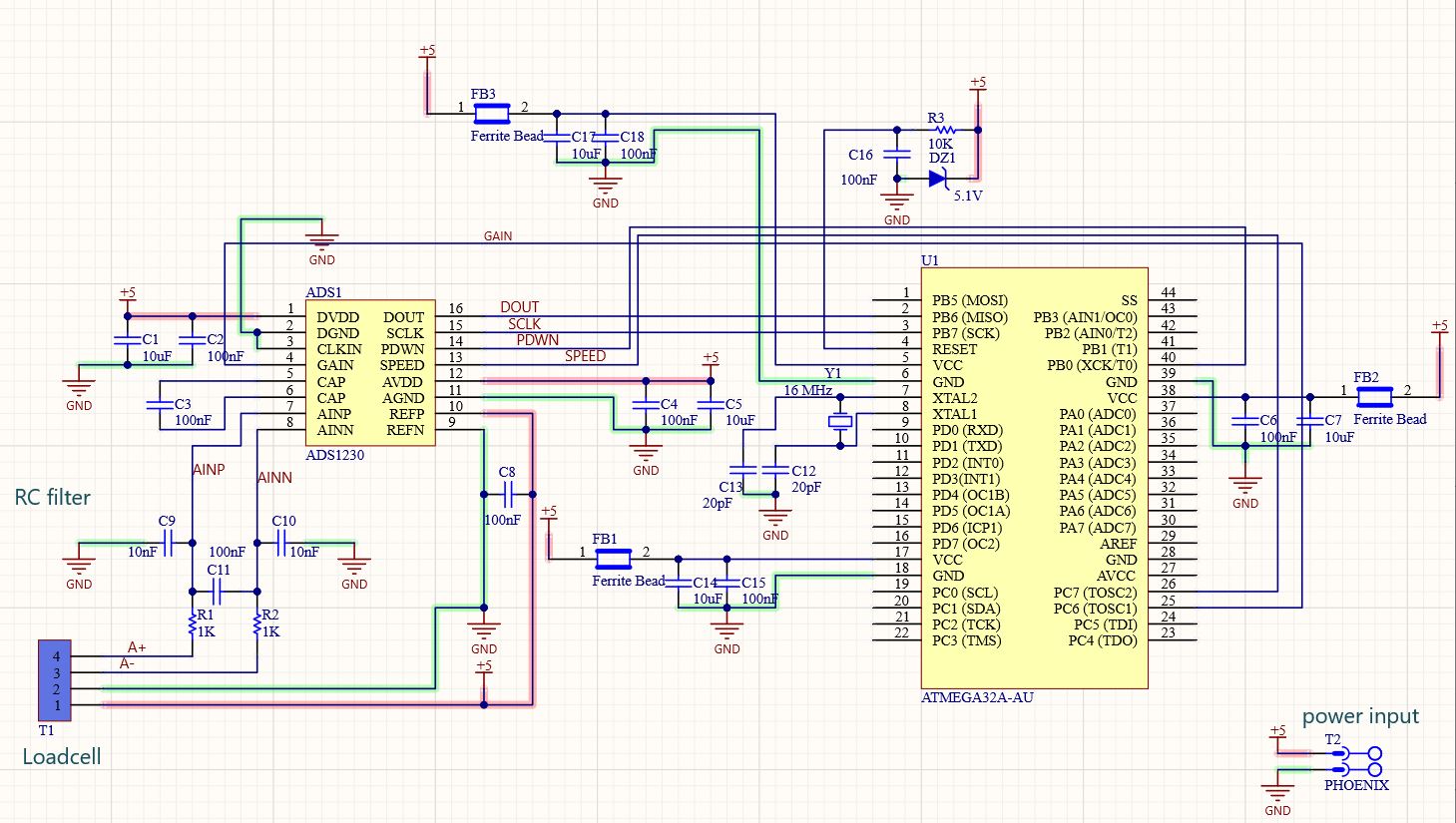
according to Bob's tips about the pcb layout and schematics for ADS1230, I have prepared a very simple schematic for a loadcell board, please find the picture below and notify me for changes if necessary, then I will prepare PCB layout and update the topic shortly.
also I have some questions:
1. is it necessary to connect AGND and DGND together? cause i had used a DC-DC isolator for analog supply and i don't want to get rid of it.
2. Shall I use decoupling capacitors for Loadcell exc+ in pin REFP?
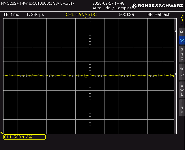
3. can I achieve 1g precision for 30 kg loadcell (2 mv/V) by gain of 64 without any noise?
regards