This thread has been locked.

If you have a related question, please click the "Ask a related question" button in the top right corner. The newly created question will be automatically linked to this question.

ADS1299: DOUT always grounded

Part Number: ADS1299

Hi,

We have implemented a design with two Daisy-chained ADS1299 and are having some issues receiving data from the second IC.

We have correctly validated the 8 channel version, but when trying to talk to the daisy chained 16 channel version, the last 8 channels data is all 0. I have checked power, and all the signals, and everything seems to be fine except that DOUT from the second ADS1299 is always 0. It seems that something is pulling it to low all the time, and no matter in which state we are this signal is 0. I have checked impedance respect ground when not trying to communicate and is not shorted.

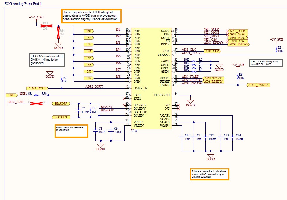
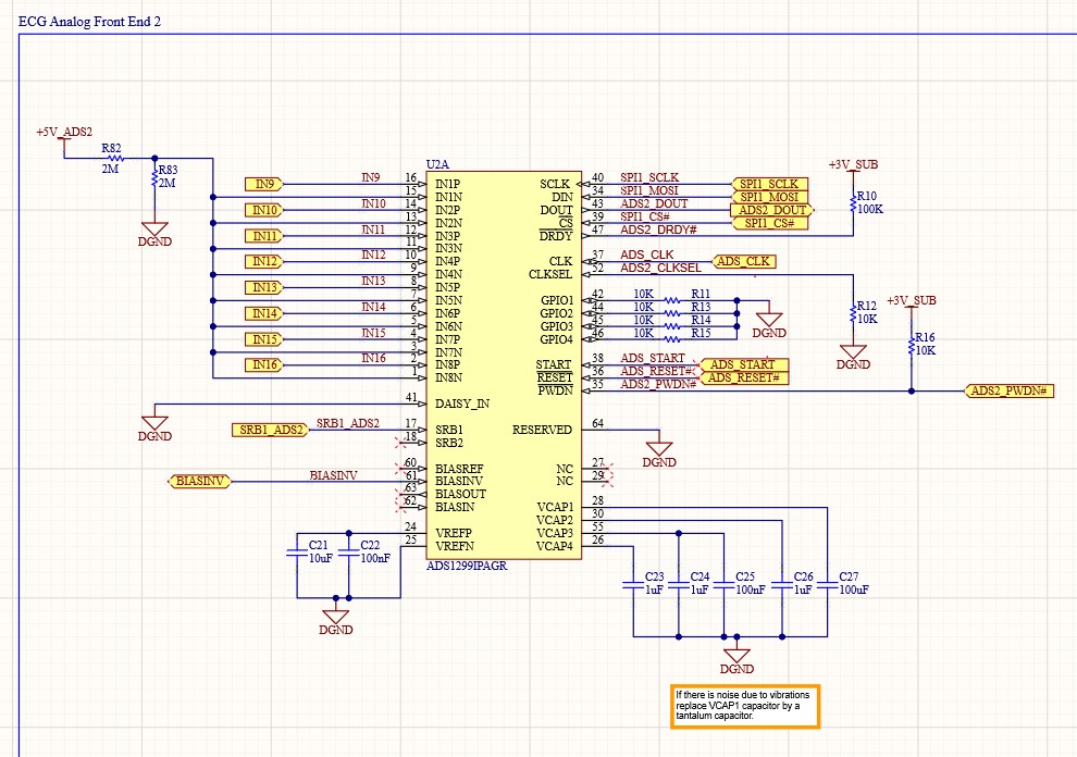
The schematics are the following, but we have removed R7 to enable the daisy chain and R82 and R83 are not assembled. 

The register configuration is the following:

app: config1: 0xB4
app: config2: 0xC0
app: config3: 0xFC
app: config4: 0x0
app: ch1set: 0x60
app: ch1set: 0x60
app: ch2set: 0x60
app: ch3set: 0x60
app: ch5set: 0x60
app: ch6set: 0x60
app: ch7set: 0x60
app: ch8set: 0x60
app: loff: 0x3
app: loffsensp: 0x0
app: loffsensn: 0x0
app: biassensp: 0xFF
app: biassensn: 0xFF
app: misc1: 0x20

Any ideas on what might be the issue or how to keep troubleshooting? We are out of ideas.

Thank you for your help.

Best regards

  • Hi,

    It looks like we have been able to avoid this issue by changing the power-up sequence. At first we were following the "Initial Flow at Power-Up" figure on page 62 of the DS and nothing was transferred from the second ADS1299 to the first one. But if we set PWDN to high before powering AVDD then the IC responds. Have you seen this issue happening before? Is there something we should change about our configuration? Can we damage the IC by setting digital signals to high before powering?

    Thank you

  • Hi Husein,

    From your design schematic, it looks like you are using an internal oscillator from the device U1A to drive the second ADS1299 (U2A). Please make sure that both devices follow the correct power-up sequence as stated in Figure 67 especially for U2A since it using the internal oscillator from U1A. I hope this helps with your debug.  

    Thanks.

    -TC 

  • Hi,

    Thank you for your prompt response. I am not sure how both devices can follow the sequence when there is only on SPI line. So right now what we are doing is power-up analog and digital supply and immediately set PDWN=1, otherwise it will not work.

    If we try to make both devices follow the sequence, we would:

    1 Powerup both devices.

    2 Wait for the oscillator of the first device to wake-up (not sure how long does that take)

    3 Set PWDN=1 for the first device

    4 Set REST=1 for both devices

    5 Wait tpor

    6 Issue Reset pulse and wait 18 tCLKs

    7 Send SDATAC Command

    8 Configure CONFIG1.CLK_EN BIT on the first ADS

    9 Wait for the oscillator on the second device to wake-up

    10 Set PWDN=1 on the second device

    ....

    Is this correct or how would you do it?

    Thank you for your help 

  • Hi Husein,

    From your schematic, you are also sharing the RESET pin for both devices. As you stated, you may have to set the PDWN=1 for both devices during power-up if you are sharing the SPI signals, and using the internal oscillator to drive the second device. It is a little tricky in this case if you cannot issue a RESET pulse to the second device separately from the first device. The second device will not get the CLK output from the first device until you set the CLK_EN bit in the CONFIG1 register. You may have to make sure all the registers in the second device are correct after it is power up and get the CLK signal from the first device.

    We recommend using the daisy-chain configuration in Figure 70b. 

    Thanks.

    -TC

  • Yes, they share the Reset pin and if I am not mistaken we are following the figure 70b configuration right? So what is your recommended power up sequence for that configuration? Should we change anything?

    Thank you

  • Hi Husein,

    I would recommend keeping the second device PWDN = 0 until the device gets the CLK signal from the first device before setting the PWDN = 1 for the second device. You will probably do not want to issue the second RESET since you are sharing the RESET which will cause the first device to turn off the CLK output. Please verify all registers setting is correct for the second device since we didn't issue the RESET sequence. 

    Thanks.

    -TC

  • Hi,

    I have the same situation, but I am unable to get proper register contents.

    Set PWDN to 0 for the second ADS

    Setup the first ADS to generate the clock (I have checked this on a scope)

    Set PWDN to 1 for the second ADS

    Send SDATAC command to second ADS

    Read ID register contents, but get 0x92 when I'm expecting 0x3E.

    Any suggestions? Do I need a reset command at some point? I can't use the reset pin as it is shared between the 2 ADS1299s.

    Regards,

    Stephen 

  • HI, we have tried your proposed solution but we keep getting all zeros. Since this is a standard Hardware configuration I understand that this is an anomaly.  We have reviewed all the routing and HW config and we don't see any errors so we suspect that it has to be a initialization issue. Is there any example code that we could test on our device to check that this is the case?

    Thank you for your help.

  • Hi Husein,

    After some discussion, the design team recommends using the daisy-chain configuration shown in Figure 70 (b). For daisy-chain configuration, it is crucial for both devices in the daisy-chain to meet the power-up sequencing described in Sec 11.1 for proper device initialization. If the power-up sequence is not met, then the device may not be operating correctly as what you are seeing. For your design configuration, it will be best to have separate RESET signals so each device can be initialized separately instead of having separate PDWNn signals.  

    Thanks.

    -TC

  • Excuse my ignorance but, are we not following the configuration shown in Figure 70(b)? We have already manufactured the system following the recommendations on the Datasheet, is there a way to initialize this system correctly?

  • Hi Husein,

    The recommended daisy-chain configuration is to clock all the daisy-chain devices with the same external CLK instead of cascading the clock from one daisy-chain device to the next. If the latter case is used, then a separate RESET signal will be the most reliable way to get all the devices in the daisy-chain to initialize properly.

    Thanks.

    -TC  

  • I see, I will try to modify our current system to try this. Is it OK if the second PWDN is set to high as soon as the ADS1299 is powered ON and stays like that during all the initialization?

    Thank you for your help

  • Hi Husein,

    If both devices receive the clock signal during power-up, then it is fine to keep the PWDN pin ramp together with the power supply with the pull-up resistor as shown in your design. 

    Thanks.

    -TC

  • If I understand correctly they do not receive the clock signal during power-up. ADS1 is using internal clock, and providing the clock to ADS2. So this is the Hardware configuration. I can try to hack the board so instead of having two separate PWDN signals we can have two resets but I have to set the second PWDN signal to high. Is that something that could work or what solutions do you think we could implement that might work?

  • Hi Husein,

    I see what you are trying to do now. Yes, it should be fine to set the ADS2 PWDN signal to high during power-up. However, the digital portion of the ADS2 device will not be initialized until CLK is present and valid. You still want to follow the power-up timing diagram in the datasheet for ADS2. 

    Thanks.

    -TC

  • I understand. You refer to the power-up diagram on the datasheet but that is for just one device and not for daisy chained device. Could you provide us with a  power-up timing diagram for a daisy chained device?

  • Hi Husein,

    The power-up timing sequence is the same for all devices. After the ADS2 gets the clock signal from the first device, you can issue a RESET pulse after tPOR or after VCAP1 is greater than 1.1V, whichever time is longer. Please refer to Note (2) in the power-up timing diagram.

    Thanks.

    -TC

  • Since both devices share the RESET signal, Issuing a RESET pulse would not reset the first device, which would turn the CLK off? 

  • Husein Gonzalez1 said:

    If I understand correctly they do not receive the clock signal during power-up. ADS1 is using internal clock, and providing the clock to ADS2. So this is the Hardware configuration. I can try to hack the board so instead of having two separate PWDN signals we can have two resets but I have to set the second PWDN signal to high. Is that something that could work or what solutions do you think we could implement that might work?

    You are making the changes to your solution to have a separate RESET for each device, aren't you? The procedure I described is intended for your new configuration where you have separate RESET control.  

  • We have manufactured the boards with the configuration shown on the schematics. Is there any initialization sequence that would allow us to boot our system correctly? Otherwise we don't have other alternative that try to hack our current boards and manufacture another batch with the new design, but for that I want to be certain that there is no way to initialize correctly with the current configuration.