This thread has been locked.

If you have a related question, please click the "Ask a related question" button in the top right corner. The newly created question will be automatically linked to this question.

DAC5662: Output volatge compliance range

Part Number: DAC5662
Other Parts Discussed in Thread: DAC5675A

Hello,

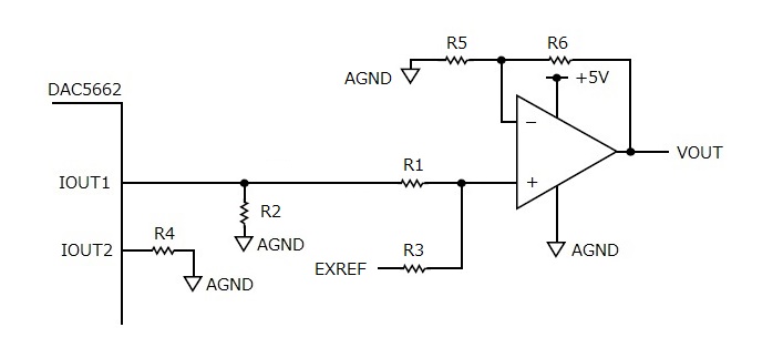
I considering interface circuit for DAC5662 using OPAMP IC.
Below circuit is current/voltage conversion circuit to convert DAC5662 output current to voltage.

The DAC5662 datasheet prescribes Output volatge compliance range of -1V to +1.25V.

I think that the output voltage of DAC5662 is calculated following formula.
I would like to check if the voltage calculated by the following formula corresponds to the output voltage compliance range.


< formula >

Output voltage of DAC5662 = IOUT1 * R1 + EXREF
(Calculation result: +0.5V to +1.0V voltage swing)

Where

IOUT1: 0mA to 10mA sine wave
R1   : 50ohm
EXREF: +0.5V


Regards,

MESH

  • No, I do not think that circuit would work.  You can reference Single-Ended Configuration on page 18 in the datasheet and also reference a couple of App Notes that discuss interfacing current source DACs to op-amps:https://www.ti.com/lit/pdf/sbaa135 and  https://www.ti.com/lit/pdf/slyt360.

    The DAC needs a resistive path to ground to set the voltage from the current source.  Once that voltage is established, then it can be amplified by the op-amp as needed.  I think your R2 needs to come before R1 to set the voltage.  R2 = 25 ohms sets the voltage at 0.5Vpp (and within compliance range) per leg.  R3 and R1 can be set to provide desired gain. R4 also set to 25 ohms.

    --RJH

  • Hello, RJ Hopper.

    Thank you for your reply.

    I thought about above circuit with reference to the contents of following materials.
    However, there is a difference in the direction of the output current from the DA converter. (sink or source)

    - Circuit of figure 4 on application report SBAA150A
    - Circuit of figure 24 (b) on DAC5675A data sheet


    I confirmed contents of your recommended materials. (SBAA135 and SLYT360)
    I think that the circuits on both materials are circuits that operate with +/- power supply operational amplifier.
    I am considering a circuit that works with a single power supply operational amplifier with adding offset voltage on input stage.
    If you know a circuit example of single supply operational amplifier circuit combined with DA converter of current source output type, please let me know.


    Regards,
    MESH

  • Understood. If needed, you can adjust the load resistor to reduce the swing slightly and then use the external reference voltage in your diagram to center at an appropriate voltage so that the swing is within the positive voltage only range of the op-amp.  You would sacrifice a bit f overall swing but could make up for it with the gain of the op-amp.

    --RJH

  • Hello, RJ Hopper.

    Thank you for your reply.

    I have 3 inquiries related this issue.

    (1) I would like to confirm that the circuit in your reply is the circuit diagram shown in the figure below.
         It is a combination of an adder circuit and a non-inverting amplifier circuit.

    (2) This is my first time to use a current output type DA converter such as DAC5662, so please check it just in case.
        50 ohm resistor is connected to the IOUT1 pin of the DAC5662 to output 20mA of full-scale current from DAC5662.
        Measure the voltage of the IOUT1 pin with reference to AGND.
        Is it okay to understand that a +1V voltage can be measured?
        Also, is it okay to understand that there is no problem if this voltage is within the compliance range?


    (3) I will perform circuit simulation with OrCAD PSPICE.
        For modeling the DAC5662, let me check if a circuit model with a current source (eg ISIN model) and a 300k ohm
        resistor connected in parallel is acceptable.
        300k ohm: Output resistance of DAC5662 on datasheet

    Regards,
    MESH

  • MESH:  Please see below.  --RJH

    (1) I don't think that you need the adder circuit.  The current source into effective 25 ohm load will set the proper common mode voltage within compliance voltage swing.

    (2) R2 should be 25 ohms (reference Single-Ended Configuration on page 18 in the datasheet) to give 0.5Vpp swing on that leg.  Since you are operating SE, half of the voltage is "wasted" in the other unused leg.

    (3) Yes that model is acceptable.  For even more basic, eliminate the 300k and just use the (ideal) current source.

  • Hello, RJ Hopper

    Thank you for your reply.
    I am starting circuit simulation based on your reply.
    I confirmed output voltage of 0.5Vpp by pull down resistor of 25 ohm on circuit simulation.

    Let me check one more thing.
    For the output voltage compliance range, which part of the DA converter should the voltage be measured and compared with the specified value of +1.25V to -1V ?

    I checked the contents of the data sheet, but I did not understand the above contents, so I would appreciate it if you could tell me.

    Regards,
    MESH

  • You can measure at the DAC output pin.  20mA max current to 25 ohm load yields 0.5Vpp on that leg.  With both legs it would 1 Vpp differential.    --RJH

  • Hello, RJ Hopper

    Thank you for your reply.

    Your replies are very helpful for me.

    Thank you for a long time.

    When adjusting circuit conditions for DAC, I will measure voltage of both legs and compare with compliance range.

    Regards,

    MESH