This thread has been locked.

If you have a related question, please click the "Ask a related question" button in the top right corner. The newly created question will be automatically linked to this question.

DAC8775: SPI communication problem with DAC8775

Part Number: DAC8775
Other Parts Discussed in Thread: DAC8771EVM,

Hi Team,

I have designed my own application board using DAC8775. Configuration and voltage levels look ok, but I am not able to read status register and see outputs on the terminals.

I am using STM32 microcontroller to communicate with DAC8775.

Below is the configuration have done in STM32 for SPI:

1. Frame format: Motorola                 2. Data size: 8 bits                         3. First bit: MSB first                 4. Prescaler: 32

5. Clock polarity: High                       6. Clock phase: 1 edge                  7. CRC calculation: Disabled    8. NSS signal type: Software

Voltages: DVDD = 5V, REFIN = 5V, VPOS_IN_A and VPOS_IN_B = 3.4V, AVDD = 12V

Please find below schematic. 

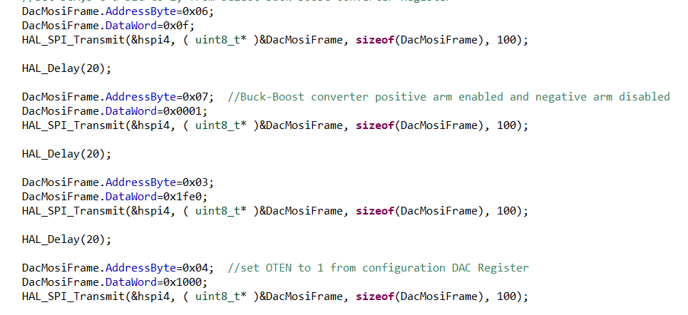
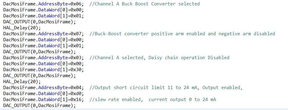
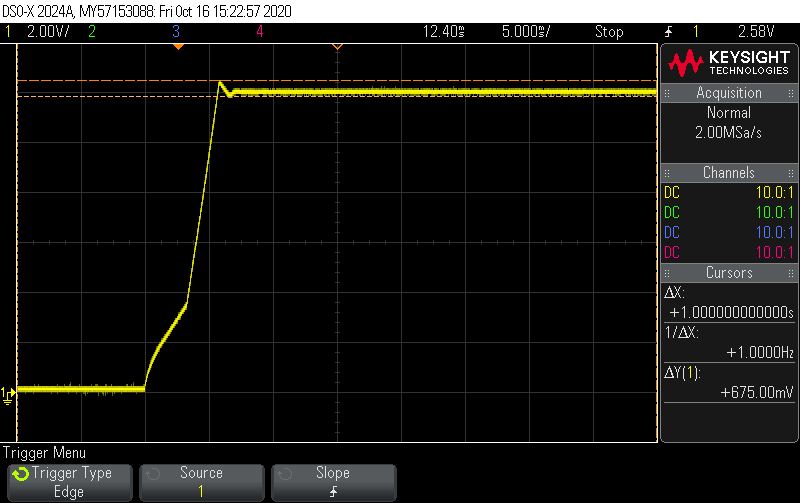
Also, please find below snapshot of configuration and waveforms:

Kindly guide me on this regard.

Than you.

Kiran

  • Hi Kiran,

    It does not seem like the image were fully embedded.  Can you just attach them to the post?

    Thanks,

    Paul

    Also, please note that many member of the DAC team are out-of-office this week, so responses will be delayed.

    Thanks,
    Paul

  • Hi Paul,

    Please find attached images.

  • Okay, thanks, I will review this and respond when I am back in the office.  Monday at the latest.

    Thanks,

    Paul

  • Problem is solved.

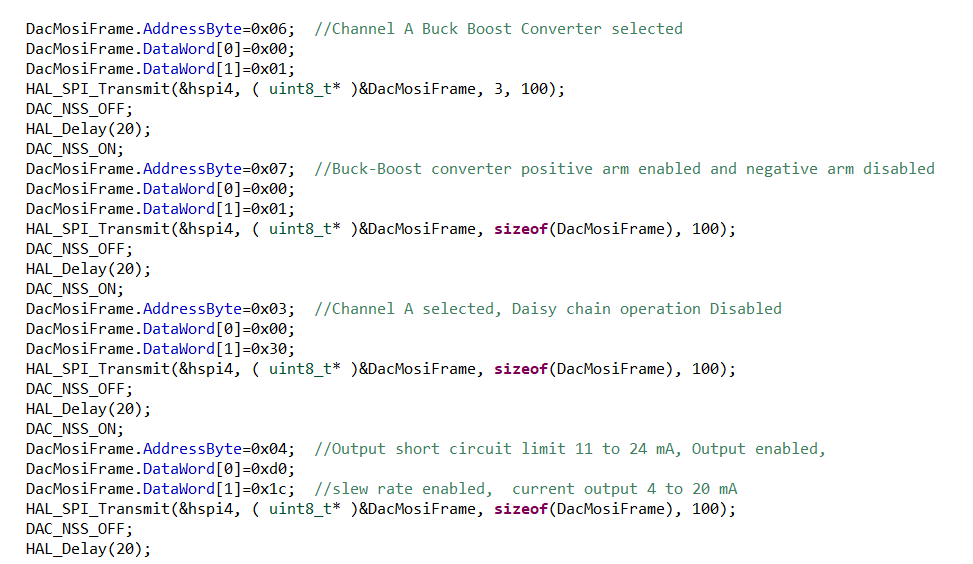
    1. The first problem was with structure. Structure contained a 16 bit data member, which was typecasted to 8 bit data by the driver. The issue was resolved by splitting the 16 bit data into an array of two 8 bit data members

    2. Controlled \SYNC signal for every write operation which was previously put permanently low for configuration and data write.

    Please find below snapshot of code.

    Thank you Paul,

    Regards,

    Kiran

  • Hi,

    Glad that your problem got solved.

    Let me know if you need any more help.

    Regards,

    AK

  • Hi,

    The board was working fine for two days. I was able to configure for 0-24 MA and able to get good results at all the current outputs.

    Abruptly, channel A and B VPOS_IN_A and VPOS_IN_B voltages started showing 0V and channel C and D VPOS_IN_C and VPOS_IN_C voltages as 3.5V.

    SPI communication is still working, but not getting any current output (0mA at all the channels).

    Any issue regarding hardware or IC (damage?).

    Regards,

    Kiran

  • Hi,

    Can you check all power supplies going into the device are within the rated values?

    I cannot comment on the device damage. These are ESD sensitive devices and therefore if you are not careful with ESD, device can damage.

    Can you please probe on the LP_x node for the non working channel and working channel and post it?

    Regards,

    AK

  • Hi,

    I got another board whose output is not working. This board also worked fine for 1 and half day. Suddenly stopped working. 

    Measured voltage at LP_x and VPOS_IN_x

    Voltages of working board : 

    (at power on without configuration)

    LP_x = 0V

    VPOS_IN_A = 3.37V

    VPOS_IN_B = 3.35V

    VPOS_IN_C = 3.34V

    VPOS_IN_D = 3.36V

    When we configure and load register values for 0-20 mA, voltages at VPOS_IN_x varies between 2.2 to 6.2V. Is this expected?

    Voltages of not working board :

    LP_x = 0V

    VPOS_IN_A = 3.57V

    VPOS_IN_B = 0.22V

    VPOS_IN_C = 3.57V

    VPOS_IN_D = 3.58V

    Also, I have observed that the temperature of IC whose output is not working is more (about 40 - 45 degree C)

    Can you find out the reason why IC is not giving current output after some time.

    Regards,

    Kiran

  • Kiran,

    I'm not sure why you're having this problem. I don't see anything in particular that you're doing wrong. I would note that if the buck-boost converter is disabled, the VPOSx value of 3.4V is normal, and that +0.23V is a normal value for VNEGx. 

    Can you able to read back all of the register values from the device just to make sure that the converter isn't shut down. Are you sure that all of the surrounding circuitry is ok? Have any of the other pins experienced any ESD or overvoltage events?

    I'll look over your schematic again and see if there's anything that I've missed.

    Joseph Wu  

  • Thanks Joseph,

    Yes, I can read back all of register values from the device.

    Status register value of 2 different boards which are not working.

    1. Status register (0x0b) = 0x1680 

    2. Status register (0x0b) = 0x1660 

    surrounding circuitry looks ok and we take care of ESD.

    I found one mistake in design. Voltage of capacitors C79,C83,C61 and C68 is 16V.

    Can this be the reason of DAC suddenly stops working analog part. 

    Regards

    Kiran

  • Kiran,

    I'm not sure if the lower voltage capacitors are the problem. With the buck boost circuitry, it's possible that the voltages could certainly exceed this value. I'm not sure if this would damage the capacitors, or simply de-rate the value with higher voltages.

    Looking at what you got from the status registers, the 0x1680 indicates that the power is good, and the 0x1660 indicates that the power is not good. Again, I don't have much idea of what could be the problem.

    There are still a couple things to try. First, for the non-working board can you power it down, and power it on again with a reset and then set a new configuration? I would set the buck-boost to positive enabled with clamp mode and set the positive clamp to +15V. You can set the negative clamp to -15V, but with the negative output disabled, it really doesn't matter. Then set the device to +10V output mode, and set the output to 5V and enable the output (which would be half-scale).

    Then measure the VPOS and VOUT With this you can check that the output and the VPOS side of the buck-boost is working. This will check to see that the buck boost can still make the conversion for the supply. With the current mode output, the auto learn may set the VPOS automatically, and here I just want to see that the buck boost can still set the output to a specific output.

    If the VPOS and VOUT is not giving a proper value, then I would try to remove the device and replace it with a new one. I understand that this could be difficult because of the package. With such a large device and large thermal pad, you may need to be careful with the heat applied (likely hot air to melt the solder) and make sure not to disturb the remaining devices nearby. By replacing the device, we can determine if this is a problem with the device or with the surrounding circuitry.


    Joseph Wu

  • Hi Joseph,

    As per your suggestion, I worked on one the board which was not working.

    Set the positive clamp to +/-15V. Configured for 0-10V and sent 5V count. I could get voltages as below. 

    VPOS_IN_A = 15.6V, Vout_A = 0V

    VPOS_IN_B = 0.22V, Vout_B = 0V

    VPOS_IN_C = 15.4V, Vout_C = 0V

    VPOS_IN_D = 15.6V, Vout_D = 0V

    Then, same exercise I did for working board for channel A. 

    I got VPOS_IN_A = 15.6V, Vout_A = 5V. working fine.

    Later, I measured resistance between VPOS_IN_B and GND after removing all external component of channel B (when no power applied). It is 7 OHM.

    For other channels, (A,C and D) it shows open. 

    I am not sure what is the problem with channel B. Internal buck boost circuit of channel A, C and D is working, but why output did not appear at the output terminal.

    And lastly how this problem has come.

    Regards,

    Kiran

  • Kiran,


    The low resistance between VPOS_IN_B and GND does imply the device is damaged. However, I don't know of any specific failure mechanisms for this device. VPOS_IN is basically the top side of the driver for the output of the DAC. I'm not sure if this means that the damage occurred at the DAC output.

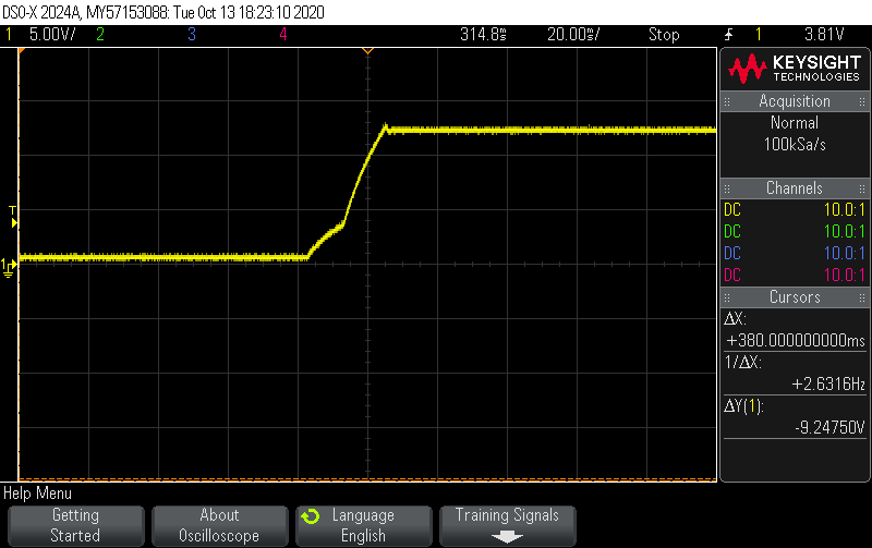
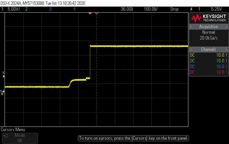
    I would look at the other channels to check the operation of the buck-boost converter. Can you use an oscilloscope to look at the ripple and the output voltage of VPOS? I would also look at the voltage and ripple at the LN node as well.

    In particular, I would look for large ripples or spiking of these voltages that might exceed the maximum ratings of the pins of the device.

    Additionally, you might have large transients at startup, so I would also look to see if there is spiking at the startup of the buck boost.

    I'll check with others that have some experience with this device. I don't know of similar failure mechanisms, but maybe others have some different experience.


    Joseph Wu

  • Thank you Joseph,

    Please find below waveforms captured.

    Ripple at 12V is about 300mV.

    PVDD

    VPOS_IN_A

    Please find below power supply. Using U23 for 12V supply to DAC8775

    Regards,

    Kiran

  • Kiran,


    Can you also plot the ripple on the scope with AC coupling? I'd like to see that as well.

    My plots for the buck-boost were a bit different. I had a more rounded startup on VPOS, and the ripple was much smaller (~50mV). I would note that I'm using the single channel DAC8771EVM for the test, but it should be the same.

    The output characteristics vary quite a bit depending on the voltage setting and output, so your ripple of 300mV isn't unexpected. I've seen plots that show that magnitude for ripple. I don't see anything unusual for the plots that you provided.

    In the damaged device, when it stopped working, what was the setting for the device? What was the DAC output range and setting? Also for the plots that you show, what is DAC output range and setting there?


    Joseph Wu

  • Hi Joseph,

    Today, I found one another non-working board (Board no. 9). Surprisingly, this time, channel 3 is damaged, but all other channels are working.  

    Channel 3 voltages: VPOS_IN_C = 1V. and Output = 0V.

    Specifically, I had put this board for cyclical testing with different loads. Test current was 24 mA. Output was ON (enable) for 10 seconds and OFF (disable) for 500 msec.

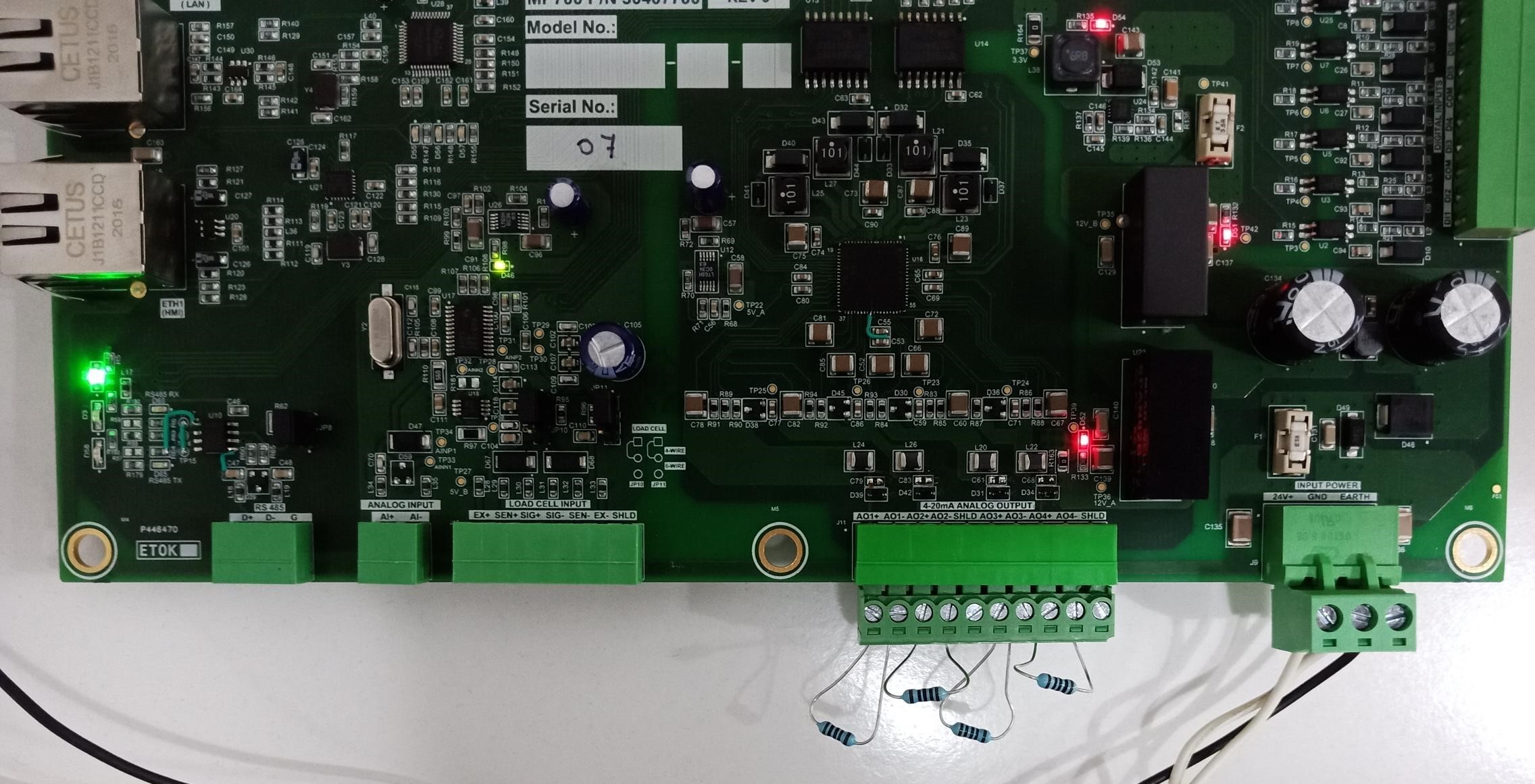
    Load connected to channels.

    Ch1 = 360 OHM

    Ch2 = 240 OHM

    Ch3 = 500 OHM

    CH4 = 120 OHM

    This particular board was working for 4 days (from 27 to 30 October) continuously. Today morning I found it's channel 3 is not working.

    Please find below description of boards failure:

    We have manufactured 10 boards in two lots 3+7.

    Board no.1: Board no. 1 was working for 1 and half day.

    One day morning (10-20 days ago) when developer started working, it was found damaged.

    Board no.3: We did not get any output at first power on.

    Board no.10: Board no 10 also was working for 1 day (all channels)

    This board found damaged, while developer was debugging the program. 

    Configuration in all the boards is same.

    1. External reference is enabled

    2. Current range 0-24 mA

    3. Buck boost converters A, B, C and D are selected.

    4. Buck-Boost converter positive arm enabled and negative arm disabled.

    5. Buck-Boost converter in full tracking mode

    Please find below waveform captured on DSO with AC coupling.

    Now I have lot may questions:

    1. Is 12V sufficient for driving the IC and all buck - boost converters (for 24mA output to all channels and full load)? 

    2. Can I use 24V instead 12V? Will it improve?

    3. Can I connect and test 12V directly to the VPOS_IN_x pins and disable buck-boost converter in the code.

    4. Board no. 9 (ch 3) is damaged due to switching of current from 0 24mA continuously. is it correct?

    5. What is the solution for this ?

    6. Shall I continue with this chip. Is  this reliable? 

    Regards,

    Kiran

  • Kiran,


    At this point, I'm not sure what happened to damage the devices on your board. I've checked with designers and other apps engineers familiar with this device and I haven't gotten any indication that this is something they've seen before. I can't give a solution for something that I don't have any answers for right now.

    For your questions, these are the answers that I have right now.

    1. The 12V should be sufficient for driving the IC and the buck-boost converter with the load. I've made of measurements on efficiency for different operating modes of the device, and I don't think that even on max current output, it shouldn't be a problem for the buck-boost.

    2. You could use a 24V supply, but I don't think that is part of the problem.

    3. You should be able to test the device by connecting the 12V supply to VPOS_IN_x, this is shown as an option in Figure 137 of the datasheet as the DAC8775 with External Supplies.

    4. I'm not sure that the device is damaged due to switching of current from 0 to 24mA continuously. I haven't heard of this happening. I'd still like to know how this test is set up. Was the device set up to to output 24mA and then the OTEN bit set high and low? If this is the failure mechanism, I'd like to know more about exactly how the device is set up.

    5. Again, I haven't been able to find any instance of this type of failure for this device, so I can't say what a solution would be at this point

    6. This device has sold many many units since its introduction, and I don't have any reason to believe that this is an unreliable device.

    I'd like to try to debug this problem with you and see if we can determine the failure mechanism. For now, I want to determine if this current output cycling is the real failure mechanism, or if this it is something else. From your description, there were two other boards that were damaged with the developers. Were they running a similar test with cycling the output current? Do you know what tests they were running when the board failed? Did they have boards with the lower voltage rated capacitors? Did replace the capacitors with the lower voltage rating (you had mentioned in a previous post that there were some capacitors with lower than expected voltage ratings)?

    For the settings, you posted a code snippet about the setup. Is this the basic sequence for enabling the device?
    In that sequence, it showed writes to 0x06 to select the correct buck-boost, then 0x07 to set the buck-boost settings. Then it shows writes to 0x03 to select the DAC, and then the write to 0x04 to configure the DAC. Are there any other settings for this device? Are there any other settings or timing that you think might be important?

    The application section of the datasheet also describes specific recommendations for values for the buck boost converter. This is described in section 9.1.1. There are values for inductors, capacitors, and diodes. Can you provide the BOM for the devices used in your schematic?

    I'm continuing to talk to our design and apps engineers here to see what the potential source of this problem is.

    Joseph Wu

  • Kiran,

    One other thing that I wanted to note about #3 is that using a external supply is possible, but you need to make sure the internal buck-boost is not enabled. There some discussion about that in the DAC8775EVM, in section 2.4.2.

    Joseph Wu

  • Thank you Joseph,

    For the cyclic test I was changing DAC counts, 0 and 65535, not OTEN bit. Configured for current output (0-24mA) mode and I was sending 65535 (24 mA) DAC count for 10 seconds and 0 DAC count for 500 msec.

     Please find below image for better understanding.

    As I wrote in last reply, two boards (board no 1 and 3) damaged while code development and third board (board no 10)  damaged while debugging program. We were trying to send constant count (mA) for all four channels. We were not doing specific test but verifying correct mA at the output by sending constant count . At that instance of time, there was no same configuration as in forth board (board no 9) which channel 3 is not working. 

    When I was testing board no 1, 3 and 10, low voltage rated capacitor were present. Now we have replaced capacitors.

    I do not think time or setting is a problem. I think ,you can suggest me by reviewing code. I have attached it below.

    Today, I connected 12V (Avdd) to VPOS_IN_x for board no. 9 and changed configuration as per external supply (disabled buck-boost). I could observe correct current and voltage outputs at all 4 channels (channel 3 also).  This means, with external supply, channel no. 3 is working in current and voltage modes and Buck boost converter of channel 3 is not working.

    So, I tried same for boards 1 and 3. But, I not did get the current and voltage output. Supply voltage drops. I think DAC of these boards is definitely damaged. 

    Also, I have put another two boards (board no 8 and 7) for cyclic testing with 100 OHM resistor load. Here I am gradually increasing current from 0 to 24 mA. These two boards are working from 30th Oct. without stop.

    Till today, I am not able to find out the reason of DAC damage. Also why buck boost converter of board no 9 (ch 3) is damaged. So, I did not start testing of board no. 2, 4, 5 and 6.  

    I have questions:

    1. Shall I continue with external supply ?

    2. Other than minimizing power dissipation, what is the use of buck boost converter, if all works with external supply?

    Please find below code to understand sequence.

    Also, please find attached BOM.

    TT20_Controller_BOM_2020_08_27.xlsx

    #define DAC_NSS_ON HAL_GPIO_WritePin(DAC_NSS_GPIO_Port,DAC_NSS_Pin,GPIO_PIN_RESET)
    #define DAC_NSS_OFF HAL_GPIO_WritePin(DAC_NSS_GPIO_Port,DAC_NSS_Pin,GPIO_PIN_SET)
    #define DAC_CLR_DISABLE HAL_GPIO_WritePin(DAC_CLR_GPIO_Port, DAC_CLR_Pin, GPIO_PIN_RESET);
    #define DAC_CLR_ENABLE HAL_GPIO_WritePin(DAC_CLR_GPIO_Port, DAC_CLR_Pin, GPIO_PIN_SET);

    void DAC_Hw_Reset(void)
    {
    HAL_GPIO_WritePin(DAC_RESET_GPIO_Port, DAC_RESET_Pin, GPIO_PIN_RESET);
    HAL_Delay(100);
    HAL_GPIO_WritePin(DAC_RESET_GPIO_Port, DAC_RESET_Pin, GPIO_PIN_SET);
    }

    void DAC_Init(void)
    {
    DacMosiFrame.AddressByte=0x06;
    DacMosiFrame.DataWord[0]=0x00;
    DacMosiFrame.DataWord[1]=0x00;
    DAC_OUTPUT(0,DacMosiFrame);

    DacMosiFrame.AddressByte=0x07;
    DacMosiFrame.DataWord[0]=0x00;
    DacMosiFrame.DataWord[1]=0x00;
    DAC_OUTPUT(0,DacMosiFrame);

    DacMosiFrame.AddressByte=0x03; //Channel A selected, Daisy chain operation Disabled
    DacMosiFrame.DataWord[0]=0x00;
    DacMosiFrame.DataWord[1]=0x30;
    DAC_OUTPUT(0,DacMosiFrame);

    DacMosiFrame.AddressByte=0x04; //Output short circuit limit 11 to 24 mA, Output enabled,
    DacMosiFrame.DataWord[0]=0xd0;
    DacMosiFrame.DataWord[1]=0x16; //slew rate enabled, current output 0 to 24 mA
    DAC_OUTPUT(0,DacMosiFrame);

    }
    uint8_t AnalogOutput(uint8_t channel,uint16_t DACcount)
    {
    //variable declaration
    uint16_t DigitalData=0;
    //code
    HAL_GPIO_WritePin(DAC_LDAC_GPIO_Port,DAC_LDAC_Pin,GPIO_PIN_SET);

    if(channel==0)
    {

    DacMosiFrame.AddressByte=0x06;
    DacMosiFrame.DataWord[0]=0x00;
    DacMosiFrame.DataWord[1]=0x00;
    DAC_OUTPUT(0,DacMosiFrame);
    HAL_Delay(20);
    DacMosiFrame.AddressByte=0x07;
    DacMosiFrame.DataWord[0]=0x00;
    DacMosiFrame.DataWord[1]=0x00;
    DAC_OUTPUT(0,DacMosiFrame);
    DacMosiFrame.AddressByte=0x03; //Channel A selected, Daisy chain operation Disabled
    DacMosiFrame.DataWord[0]=0x00;
    DacMosiFrame.DataWord[1]=0x30;
    DAC_OUTPUT(0,DacMosiFrame);
    HAL_Delay(20);
    DacMosiFrame.AddressByte=0x04; //Output short circuit limit 11 to 24 mA, Output enabled,
    DacMosiFrame.DataWord[0]=0xd0;
    DacMosiFrame.DataWord[1]=0x16; //current output 0 to 24 mA
    DAC_OUTPUT(0,DacMosiFrame);
    }

    else if(channel==1)
    {


    DacMosiFrame.AddressByte=0x06;
    DacMosiFrame.DataWord[0]=0x00;
    DacMosiFrame.DataWord[1]=0x00;
    DAC_OUTPUT(0,DacMosiFrame);
    HAL_Delay(20);
    DacMosiFrame.AddressByte=0x07;
    DacMosiFrame.DataWord[0]=0x00;
    DacMosiFrame.DataWord[1]=0x00;
    DAC_OUTPUT(0,DacMosiFrame);
    DacMosiFrame.AddressByte=0x03; //Channel B selected, Daisy chain operation Disabled
    DacMosiFrame.DataWord[0]=0x00;
    DacMosiFrame.DataWord[1]=0x50;
    DAC_OUTPUT(0,DacMosiFrame);
    HAL_Delay(20);
    DacMosiFrame.AddressByte=0x04; //Output short circuit limit 11 to 24 mA, Output enabled,
    DacMosiFrame.DataWord[0]=0xd0;
    DacMosiFrame.DataWord[1]=0x16; //current output 0 to 24 mA
    DAC_OUTPUT(0,DacMosiFrame);

    }

    else if(channel==2)
    {

    DacMosiFrame.AddressByte=0x06;
    DacMosiFrame.DataWord[0]=0x00;
    DacMosiFrame.DataWord[1]=0x00;
    DAC_OUTPUT(0,DacMosiFrame);
    HAL_Delay(20);
    DacMosiFrame.AddressByte=0x07;
    DacMosiFrame.DataWord[0]=0x00;
    DacMosiFrame.DataWord[1]=0x00;
    DAC_OUTPUT(0,DacMosiFrame);
    DacMosiFrame.AddressByte=0x03; //Channel C selected, Daisy chain operation Disabled
    DacMosiFrame.DataWord[0]=0x00;
    DacMosiFrame.DataWord[1]=0x90;
    DAC_OUTPUT(0,DacMosiFrame);
    HAL_Delay(20);
    DacMosiFrame.AddressByte=0x04; //Output short circuit limit 11 to 24 mA, Output enabled,
    DacMosiFrame.DataWord[0]=0xd0;
    DacMosiFrame.DataWord[1]=0x16; //current output 0 to 24 mA
    DAC_OUTPUT(0,DacMosiFrame);

    }

    else if(channel==3)
    {
    DacMosiFrame.AddressByte=0x06;
    DacMosiFrame.DataWord[0]=0x00;
    DacMosiFrame.DataWord[1]=0x00;
    DAC_OUTPUT(0,DacMosiFrame);
    HAL_Delay(20);
    DacMosiFrame.AddressByte=0x07;
    DacMosiFrame.DataWord[0]=0x00;
    DacMosiFrame.DataWord[1]=0x00;
    DAC_OUTPUT(0,DacMosiFrame);
    DacMosiFrame.AddressByte=0x03; //Channel D selected, Daisy chain operation Disabled
    DacMosiFrame.DataWord[0]=0x01;
    DacMosiFrame.DataWord[1]=0x10;
    DAC_OUTPUT(0,DacMosiFrame);
    HAL_Delay(20);
    DacMosiFrame.AddressByte=0x04; //Output short circuit limit 11 to 24 mA, Output enabled,
    DacMosiFrame.DataWord[0]=0xd0;
    DacMosiFrame.DataWord[1]=0x16; //current output 0 to 24 mA
    DAC_OUTPUT(0,DacMosiFrame);
    }

    else
    {

    }

    DacMosiFrame.AddressByte=0x05;
    DacMosiFrame.DataWord[0]=(DACcount>>8);
    DacMosiFrame.DataWord[1]=(uint8_t)DACcount&0xff;
    DAC_OUTPUT(0,DacMosiFrame);
    HAL_GPIO_WritePin(DAC_LDAC_GPIO_Port, DAC_LDAC_Pin, GPIO_PIN_RESET);

    //read DAC Data Register

    DacMosiFrame.AddressByte=0x85;
    DacMosiFrame.DataWord[0]=0x00;
    DacMosiFrame.DataWord[1]=0x00;
    DAC_OUTPUT(1,DacMosiFrame);
    HAL_Delay(20);
    DAC_OUTPUT(1,DacMosiFrame);

    //read DAC status Register

    DacMosiFrame.AddressByte=0x8b;
    DacMosiFrame.DataWord[0]=0x00;
    DacMosiFrame.DataWord[1]=0x00;
    DAC_OUTPUT(1,DacMosiFrame);
    HAL_Delay(20);
    DAC_OUTPUT(1,DacMosiFrame);


    DigitalData=(((DacMisoFrame.DataWord[0])<<8)|DacMisoFrame.DataWord[1]);

    if(DigitalData==DACcount)
    return(0);
    else
    return(1);
    }

    int main(void)
    {
    /* USER CODE BEGIN 1 */

    /* USER CODE END 1 */

    /* MCU Configuration--------------------------------------------------------*/

    /* Reset of all peripherals, Initializes the Flash interface and the Systick. */
    HAL_Init();

    /* USER CODE BEGIN Init */
    /* USER CODE END Init */

    /* Configure the system clock */
    SystemClock_Config();

    /* USER CODE BEGIN SysInit */

    /* USER CODE END SysInit */

    /* Initialize all configured peripherals */
    MX_GPIO_Init();
    MX_SPI4_Init();
    /* USER CODE BEGIN 2 */
    DAC_Hw_Reset();
    DAC_CLR_DISABLE;

    DAC_Init();

    DAC_Count=0x0000;
    /* USER CODE END 2 */

    /* Infinite loop */
    /* USER CODE BEGIN WHILE */
    while (1)
    {
    /* USER CODE END WHILE */

    /* USER CODE BEGIN 3 */

    //AnalogOutput(0,DAC_Count);
    //AnalogOutput(1,DAC_Count);
    //AnalogOutput(2,DAC_Count);
    //AnalogOutput(3,DAC_Count);
    //HAL_Delay(500);
    //DAC_Count=DAC_Count+5461;

         HAL_GPIO_TogglePin(LED1_GPIO_Port, LED1_Pin);

        
         DAC_Count=0xffff;             // ch1 on
         AnalogOutput(0,DAC_Count);
         AnalogOutput(1,DAC_Count);
         AnalogOutput(2,DAC_Count);
         AnalogOutput(3,DAC_Count);
         HAL_Delay(10000);
         HAL_GPIO_TogglePin(LED1_GPIO_Port, LED1_Pin);

         DAC_Count=0x0000;             //ch1 off
         AnalogOutput(0,DAC_Count);
         HAL_Delay(500);

         AnalogOutput(1,DAC_Count);
         HAL_Delay(500);
         HAL_GPIO_TogglePin(LED1_GPIO_Port, LED1_Pin);
        
         DAC_Count=0xffff;             //ch2 on
         AnalogOutput(1,DAC_Count);
        
         AnalogOutput(0,DAC_Count);
         HAL_Delay(2000);
    //--------------------------------------------------------------

         DAC_Count=0x0000;             //ch3 off
         AnalogOutput(2,DAC_Count);
         AnalogOutput(3,DAC_Count);
         HAL_Delay(500);
         HAL_GPIO_TogglePin(LED1_GPIO_Port, LED1_Pin);

    //----------------------------------------------------------------
         DAC_Count=0xffff;             // ch3 on
         AnalogOutput(2,DAC_Count);
        
         AnalogOutput(3,DAC_Count);
         HAL_Delay(10000);
         HAL_GPIO_TogglePin(LED1_GPIO_Port, LED1_Pin);
    }
     /* USER CODE END 3 */
    }
  • Kiran,


    It will take a while for me to read through the code and check over the order of operation, so it may take another day to get back to you. I did have a few other follow up questions.

    Just to keep everything clear, boards 1, 3, and 10 were damaged while debugging the board and happened to have some low voltage rated caps. For these damaged boards, do all of them show a short from VPOS_IN_B to GND? I want to see if all of these boards have the same failure mechanism. Also, did all of these fail the B channel? For these boards, they were only sending out a static output current without changing the IOUT value.

    For board #9, this board failed channel C and this was testing with alternating periods of full scale and zero scale output (with about a 95% duty cycle) when using the buck-boost. Do you feel like this is a different failure mechanism? Have you checked the resistance from VPOS_IN_C to GND? If the failure mechanism is the same, I would have guessed that using an external supply wouldn't help because the supply would have been dragged down.

    However, if you're able to use the external supply it would seem to imply that the DAC is still operating and that the channel C buck-boost had failed. If you need to, you could still use this to evaluate the device, but, I'd still like to debug this problem. However, I would point out that if boards 1 and 3 have the same short from VPOS_IN_B to GND, this would affect the operation of the DAC if the external supply can't maintain power, and it might not be the DAC that has the problem. You could check to see how much current the external supply is pulling out.

    Also, would you be able to remove a damaged device from a board and send it to me? I'd like to test it and see what functionality I could test out of the damaged device. 

    I've sent you a friend request through the E2E forum. You should receive a notification and you can add me as a friend. This way we can exchange messages directly and you can send the full schematic without posting it publicly.

    Again, I'll try to review your code and other comments in the post tomorrow.


    Joseph Wu

  • Thanks Joseph,

    All of them do not show a short from VPOS_IN_B to GND and not observed same failure mechanism.

    In boards 1,3 and 10, all the channels have failed.

    In board no 9, I observed different failure mechanism.  

    Resistance between VPOS_IN_x to GND for CH 3 (boards no 9) is 470 OHM and other at terminals VPOS_IN_A_B_D to GND is 1.7 M OHM.

    I have checked 12V supply by disconnecting DAC and connecting external load. It is working fine. 

    Yes, I will definitely send devices to you for instigation.

    I tried to send private message, but failed. First I typed your name in recipient text box. If I go to subject text box, your name vanishes from recipient text box.

    Regards,

    Kiran

  • Hi Kiran,

    My understanding is that you are communicating with Joe over messages/email. I am going to close the thread for now.

    Thanks,

    Paul

  • Thank you Paul,

    Yes. You can close the thread.

    Regards,

    Kiran