Other Parts Discussed in Thread: ADS1299
Hello everyone!
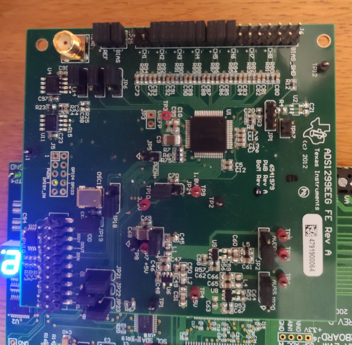
I'm currently working on a BCI application using the ADS1299EEGFE-PDK to acquire the EEG signals. In my current setup I'm using an Arduino UNO to interface with the Daughter card via SPI, while the MMB0 is used only as a power supply.
The GPIO pins are connected as follows (the jumpers on the daughter card are left in default settings)
----------------------------------------------------------------------
Arduino UNO <----> ADS1299
- SCLK [pin 13] <----> CLK [J3.3]
- MISO [pin 12] <----> DOUT [J3.13]
- MOSI [pin 11] <----> DIN [J3.11]
- SS [pin 10] <----> CS [J3.7]
- DRDY [pin 9] <----> DRDY [J3.15]
- GND [pin 14] <----> GND [J3.4]
----------------------------------------------------------------------
The sketch I'm using is an example from the library ADS1299 for Arduino which should read and write to some registers:
#include <ADS1299.h>

ADS1299 ADS;

//Arduino Uno - Pin Assignments; Need to use ICSP for later AVR boards
// SCK = 13
// MISO [DOUT] = 12
// MOSI [DIN] = 11
// CS = 10;
// DRDY = 9;

//  0x## -> Arduino Hexadecimal Format
//  0b## -> Arduino Binary Format

boolean deviceIDReturned = false;
boolean startedLogging = false;

void setup() {

  Serial.begin(115200);
  Serial.println();
  Serial.println("ADS1299-bridge has started!");

  ADS.setup(9, 10); // (DRDY pin, CS pin);
  delay(10);  //delay to ensure connection

  ADS.RESET();
}

void loop(){

  if(deviceIDReturned == false){

    ADS.getDeviceID(); //Funciton to return Device ID

    //prints dashed line to separate serial print sections
    Serial.println("----------------------------------------------");

    //Read ADS1299 Register at address 0x00 (see Datasheet pg. 35 for more info on SPI commands)
    ADS.RREG(0x00);
    Serial.println("----------------------------------------------");

    //PRINT ALL REGISTERS... Read 0x17 addresses starting from address 0x00 (these numbers can be replaced by binary or integer values)
    ADS.RREG(0x00, 0x17);
    Serial.println("----------------------------------------------");

    //Write register command (see Datasheet pg. 38 for more info about WREG)
    ADS.WREG(CONFIG1, 0b11010110);
    Serial.println("----------------------------------------------");

    //Repeat PRINT ALL REGISTERS to verify that WREG changed the CONFIG1 register
    ADS.RREG(0x00, 0x17);
    Serial.println("----------------------------------------------");

    //Start data conversions command
    ADS.START(); //must start before reading data continuous
    deviceIDReturned = true;
  }

  //print data to the serial console for only the 1st 10seconds of
  while(millis()<10000){
    if(startedLogging == false){
      Serial.print("Millis: "); //this is to see at what time the data starts printing to check for timing accuracy (default sample rate is 250 sample/second)
      Serial.println(millis());
      startedLogging = true;
    }

    //Print Read Data Continuous (RDATAC) to Ardiuno serial monitor...
    //The timing of this method is not perfect yet. Some data is getting lost
    //and I believe its due to the serial monitor taking too much time to print data and not being ready to recieve to packets
    ADS.updateData();
  }


}
Which returned the following output in the serial monitor:
ADS1299-bridge has started!
0
----------------------------------------------
ID, 0x00, 0x00, 0, 0, 0, 0, 0, 0, 0, 0
----------------------------------------------
ID, 0x00, 0x00, 0, 0, 0, 0, 0, 0, 0, 0
CONFIG1, 0x01, 0x00, 0, 0, 0, 0, 0, 0, 0, 0
CONFIG2, 0x02, 0x00, 0, 0, 0, 0, 0, 0, 0, 0
CONFIG3, 0x03, 0x00, 0, 0, 0, 0, 0, 0, 0, 0
LOFF, 0x04, 0x00, 0, 0, 0, 0, 0, 0, 0, 0
CH1SET, 0x05, 0x00, 0, 0, 0, 0, 0, 0, 0, 0
CH2SET, 0x06, 0x00, 0, 0, 0, 0, 0, 0, 0, 0
CH3SET, 0x07, 0x00, 0, 0, 0, 0, 0, 0, 0, 0
CH4SET, 0x08, 0x00, 0, 0, 0, 0, 0, 0, 0, 0
CH5SET, 0x09, 0x00, 0, 0, 0, 0, 0, 0, 0, 0
CH6SET, 0x0A, 0x00, 0, 0, 0, 0, 0, 0, 0, 0
CH7SET, 0x0B, 0x00, 0, 0, 0, 0, 0, 0, 0, 0
CH8SET, 0x0C, 0x00, 0, 0, 0, 0, 0, 0, 0, 0
BIAS_SENSP, 0x0D, 0x00, 0, 0, 0, 0, 0, 0, 0, 0
BIAS_SENSN, 0x0E, 0x00, 0, 0, 0, 0, 0, 0, 0, 0
LOFF_SENSP, 0x0F, 0x00, 0, 0, 0, 0, 0, 0, 0, 0
LOFF_SENSN, 0x10, 0x00, 0, 0, 0, 0, 0, 0, 0, 0
LOFF_FLIP, 0x11, 0x00, 0, 0, 0, 0, 0, 0, 0, 0
LOFF_STATP, 0x12, 0x00, 0, 0, 0, 0, 0, 0, 0, 0
LOFF_STATN, 0x13, 0x00, 0, 0, 0, 0, 0, 0, 0, 0
GPIO, 0x14, 0x00, 0, 0, 0, 0, 0, 0, 0, 0
MISC1, 0x15, 0x00, 0, 0, 0, 0, 0, 0, 0, 0
MISC2, 0x16, 0x00, 0, 0, 0, 0, 0, 0, 0, 0
CONFIG4, 0x17, 0x00, 0, 0, 0, 0, 0, 0, 0, 0
----------------------------------------------
Register 0x1 modified.
----------------------------------------------
ID, 0x00, 0x00, 0, 0, 0, 0, 0, 0, 0, 0
CONFIG1, 0x01, 0x00, 0, 0, 0, 0, 0, 0, 0, 0
CONFIG2, 0x02, 0x00, 0, 0, 0, 0, 0, 0, 0, 0
CONFIG3, 0x03, 0x00, 0, 0, 0, 0, 0, 0, 0, 0
LOFF, 0x04, 0x00, 0, 0, 0, 0, 0, 0, 0, 0
CH1SET, 0x05, 0x00, 0, 0, 0, 0, 0, 0, 0, 0
CH2SET, 0x06, 0x00, 0, 0, 0, 0, 0, 0, 0, 0
CH3SET, 0x07, 0x00, 0, 0, 0, 0, 0, 0, 0, 0
CH4SET, 0x08, 0x00, 0, 0, 0, 0, 0, 0, 0, 0
CH5SET, 0x09, 0x00, 0, 0, 0, 0, 0, 0, 0, 0
CH6SET, 0x0A, 0x00, 0, 0, 0, 0, 0, 0, 0, 0
CH7SET, 0x0B, 0x00, 0, 0, 0, 0, 0, 0, 0, 0
CH8SET, 0x0C, 0x00, 0, 0, 0, 0, 0, 0, 0, 0
BIAS_SENSP, 0x0D, 0x00, 0, 0, 0, 0, 0, 0, 0, 0
BIAS_SENSN, 0x0E, 0x00, 0, 0, 0, 0, 0, 0, 0, 0
LOFF_SENSP, 0x0F, 0x00, 0, 0, 0, 0, 0, 0, 0, 0
LOFF_SENSN, 0x10, 0x00, 0, 0, 0, 0, 0, 0, 0, 0
LOFF_FLIP, 0x11, 0x00, 0, 0, 0, 0, 0, 0, 0, 0
LOFF_STATP, 0x12, 0x00, 0, 0, 0, 0, 0, 0, 0, 0
LOFF_STATN, 0x13, 0x00, 0, 0, 0, 0, 0, 0, 0, 0
GPIO, 0x14, 0x00, 0, 0, 0, 0, 0, 0, 0, 0
MISC1, 0x15, 0x00, 0, 0, 0, 0, 0, 0, 0, 0
MISC2, 0x16, 0x00, 0, 0, 0, 0, 0, 0, 0, 0
CONFIG4, 0x17, 0x00, 0, 0, 0, 0, 0, 0, 0, 0
----------------------------------------------
Millis: 224
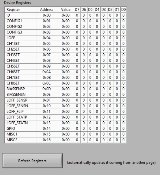
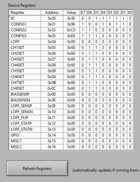
Unfortunately the data retrieved via SPI have all been zeros in all registers, and after going through all threads I could find on this topic, none seemed to help. At the current moment I don't have access to a logic analyzer or probing equipment, I just hope the error is due to a newbie mistake in the hardware connections I made.
I will be very grateful for any suggestion you could give me!
L.G.


